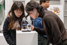
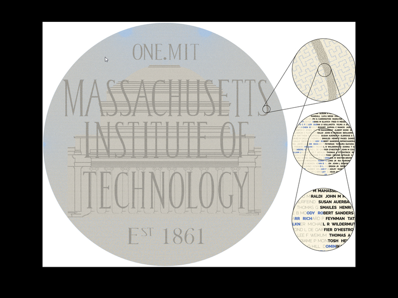

In MIT.nano’s laboratories, researchers use silicon wafers as the platform to shape transformative technologies such as quantum circuitry, microfluidic devices, or energy-harvesting structures. But these substrates can also serve as a canvas for an artist, as MIT Professor W. Craig Carter demonstrates in the latest One.MIT mosaic.
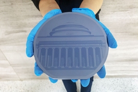
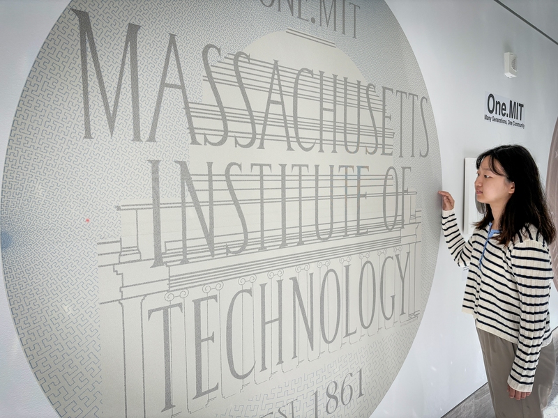
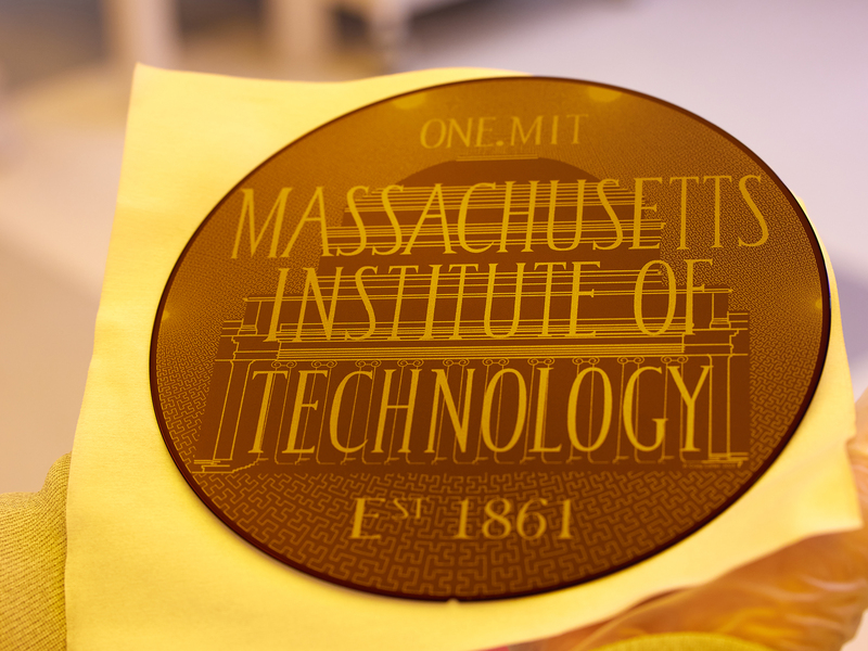
The One.MIT project celebrates the people of MIT by using the tools of MIT.nano to etch their collective names, arranged as a mosaic by Carter, into a silicon wafer just 8 inches in diameter. The latest edition of One.MIT — including 339,537 names of students, faculty, staff, and alumni associated with MIT from 1861 to September 2023 — is now on display in the ground-floor galleries at MIT.nano in the Lisa T. Su Building (Building 12).
“A spirit of innovation and a relentless drive to solve big problems have permeated the campus in every decade of our history. This passion for discovery, learning, and invention is the thread connecting MIT’s 21st-century family to our 19th-century beginnings and all the years in between,” says Vladimir Bulović, director of MIT.nano and the Fariborz Maseeh Chair in Emerging Technology. “One.MIT celebrates the MIT ethos and reminds us that no matter when we came to MIT, whatever our roles, we all leave a mark on this remarkable community.”
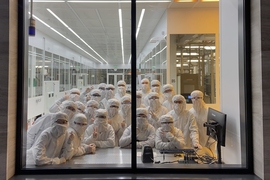
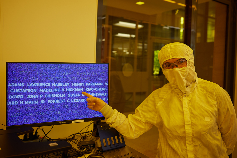
A team of students, faculty, staff, and alumni inscribed the design on the wafer inside the MIT.nano cleanrooms. Because the names are too small to be seen with the naked eye — they measure only microns high on the wafer — the One.MIT website allows anyone to look up a name and find its location in the mosaic.
Finding inspiration in the archives
The first two One.MIT art pieces, created in 2018 and 2020, were inscribed in silicon wafers 6 inches in diameter, slightly smaller than the latest art piece, which benefited from the newest MIT.nano tools that can fabricate 8-inch wafers. The first designs form well-known, historic MIT images: the Great Dome (2018) and the MIT seal (2020).
Carter, who is the Toyota Professor of Materials Processing and professor of materials science and engineering, created the designs and algorithms for each version of One.MIT. He started a search last summer for inspiration for the 2024 design. “The image needed to be iconic of MIT,” says Carter, “and also work within the constraints of a large-scale mosaic.”
Carter ultimately found the solution within the Institute Archives, in the form of a lithograph used on the cover of a program for the 1916 MIT rededication ceremony that celebrated the Institute’s move from Boston to Cambridge on its 50th anniversary.
Incorporating MIT nerdiness
Carter began by creating a black-and-white image, redrawing the lithograph’s architectural features and character elements. He recreated the kerns (spaces) and the fonts of the letters as algorithmic geometric objects.
The color gradient of the sky behind the dome presented a challenge because only two shades were available. To tackle this issue and impart texture, Carter created a Hilbert curve — a hierarchical, continuous curve made by replacing an element with a combination of four elements. Each of these four elements are replaced by another four elements, and so on. The resulting object is like a fractal — the curve changes shape as it goes from top to bottom, with 90-degree turns throughout.
“This was an opportunity to add a fun and ‘nerdy’ element — fitting for MIT,” says Carter.
To achieve both the gradient and the round wafer shape, Carter morphed the square Hilbert curve (consisting of 90-degree angles) into a disk shape using Schwarz-Christoffel mapping, a type of conformal mapping that can be used to solve problems in many different domains.
“Conformal maps are lovely convergences of physics and engineering with mathematics and geometry,” says Carter.
Because the conformal mapping is smooth and also preserves the angles, the square’s corners produce four singular points on the circle where the Hilbert curve’s line segments shrink to a point. The location of the four points in the upper part of the circle “squeezes” the curve and creates the gradient (and the texture of the illustration) — dense-to-sparse from top-to-bottom.
The final mosaic is made up of 6,476,403 characters, and Carter needed to use font and kern types that would fill as much of the wafer’s surface as possible without having names break up and wrap around to the next line. Carter’s algorithm alleviated this problem, at least somewhat, by searching for names that slotted into remaining spaces at the end of each row. The algorithm also performed an optimization over many different choices for the random order of the names.
Finding — and wrangling — hundreds of thousands of names
In addition to the art and algorithms, the foundation of One.MIT is the extensive collection of names spanning more than 160 years of MIT. The names reflect students, alumni, faculty, and staff — the wide variety of individuals who have always formed the MIT community.
Annie Wang, research scientist and special projects coordinator for MIT.nano, again played an instrumental role in collecting the names for the project, just as she had for the 2018 and 2020 versions. Despite her experience, collating the names to construct the newest edition still presented several challenges, given the variety of input sources to the dataset and the need to format names in a consistent manner.
“Both databases and OCR-scanned text can be messy,” says Wang, referring to the electronic databases and old paper directories from which names were sourced. “And cleaning them up is a lot of work.”
Many names were listed in multiple places, sometimes spelled or formatted differently across sources. There were very short first and last names, very long first and last names — and also a portion of names in which more than one person had nearly identical names. And some groups are simply hard to find in the records. “One thing I wish we had,” comments Wang, “is a list of long-term volunteers at MIT who contribute so much but aren’t reflected in the main directories.”
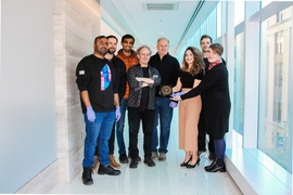
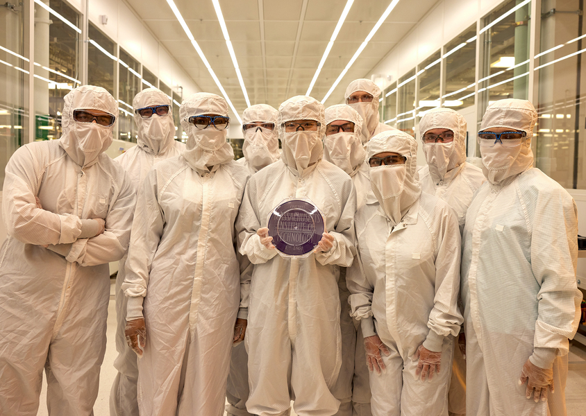
Once the design was completed, Carter and Wang handed off a CAD file to Jorg Scholvin, associate director of fabrication at MIT.nano. Scholvin assembled a team that reflected One.MIT — students, faculty, staff, and alumni — and worked with them to fabricate the wafer inside MIT.nano’s cleanroom. The fab team included Carter; undergraduate students Akorfa Dagadu, Sean Luk, Emilia K. Szczepaniak, Amber Velez, and twin brothers Juan Antonio Luera and Juan Angel Luera; MIT Sloan School of Management EMBA student Patricia LaBorda; staff member Kevin Verrier of MIT Facilities; and alumnae Madeline Hickman '11 and Eboney Hearn '01, who is also the executive director of MIT Introduction to Technology, Engineering and Science (MITES).