

Jorg Scholvin ’00, MEng ’01, PhD ’06 first set foot in a cleanroom midway through his undergraduate studies. It was the late 1990s and, as a computer science major, he’d registered for a fabrication class for a firsthand look at how a computer is assembled. “It’s amazing to see how it’s built,” he realized, “and to build it myself.” By the end of the semester, Scholvin had shifted his focus toward electrical engineering and went on to spend several years at MIT developing his fabrication skills in the Microsystems Technologies Laboratories.
Now, he guides others through all the possibilities of the cleanroom as an assistant director at MIT.nano, the Institute’s center for nanoscale science and engineering.
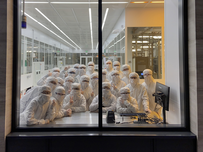
Originally from Germany, Scholvin has made MIT his home base for more than 25 years, minus a brief interlude in finance. “While being in one place, you ultimately still get to experience very different versions of it,” he says of his life on campus as an undergrad, grad student, postdoc, and staff member. Since joining MIT.nano in 2018, the year it opened, he has helped establish a new resource for campus research: a place where everything needed for nanoscale R&D is located under one roof. MIT.nano’s tools are open to the entire MIT community, as well as external users. But no matter where they come from, all those who bring their work through its doors have access to expert support from Scholvin and his colleagues.
Exploring the byways
During his undergrad years, Scholvin says, cleanrooms were primarily a place for building transistors. His doctoral research focused on transistor technology for high frequency power applications, and he collaborated with IBM on new design approaches for such devices. Over the past few decades, researchers at MIT and elsewhere have stretched the boundaries of nanoscale fabrication in many other directions. “The semiconductor industry creates a highway where things are moving at great ease and efficiency,” Scholvin says. “In the academic world, you're exploring what's to the left and the right of that highway. You're taking all the little roads and trying to see at what point could that little road, again, contribute to this whole advancement.”
Often that happens at the intersections of disciplines. Scholvin experienced that himself during his postdoctoral research in MIT’s Synthetic Neurobiology Group led by Ed Boyden, the Y. Eva Tan Professor in Neurotechnology. While Scholvin developed ways to construct new kinds of neural recording electrodes, his teammates investigated uses for these probes in brain research and medicine. Together, they used National Institutes of Health funding to spin the technology into a startup — Neural Dynamics Technologies.
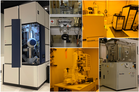
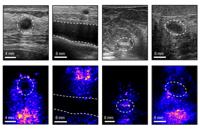
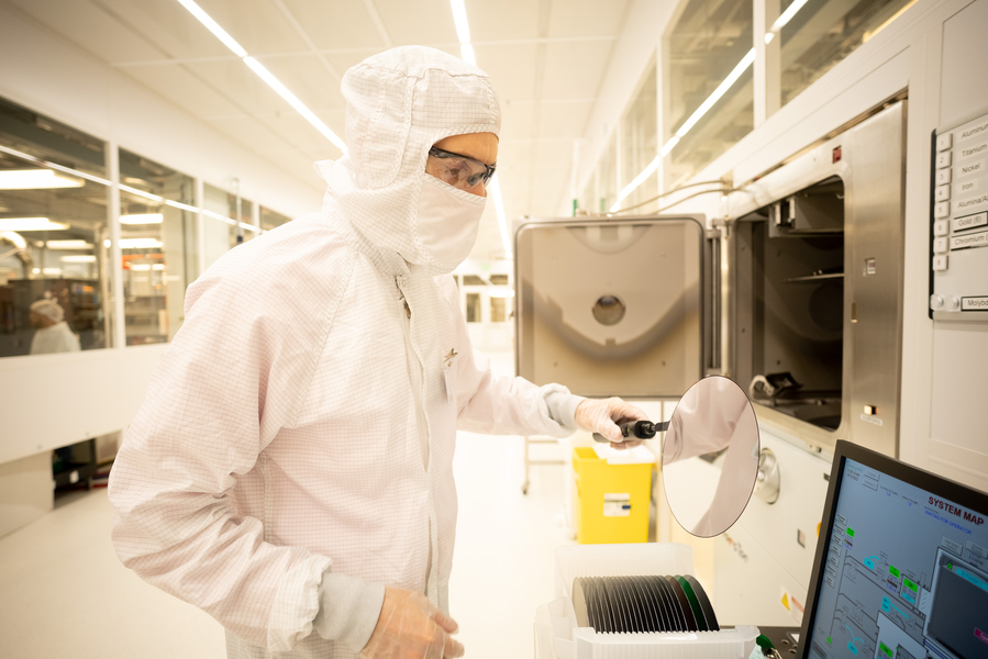
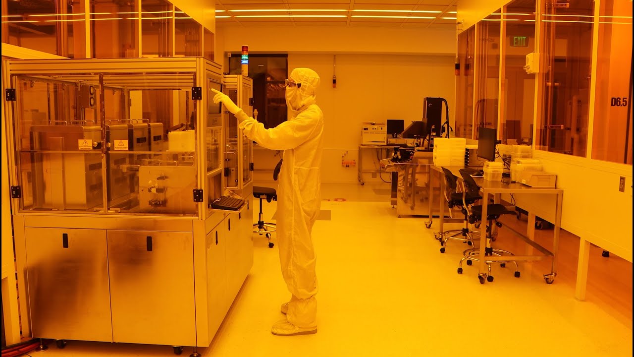
These days he shares his expertise with users from more than 50 MIT departments, labs, and centers, as well as external groups. Scholvin and his fellow instrument specialists consult with researchers to estimate the time and expense their goals entail, and to identify which among the 50 or so major fabrication instruments at MIT.nano will get the job done. That suite of tools (aka Fab.nano) enables the precise engineering of nanoscale structures and the packaging of those results within prototype devices. Fab.nano’s tool set often overlaps with or complements tools for characterization (overseen at MIT.nano by Assistant Director Anna Osherov), which can be used to assess and analyze the properties of such structures.
“As director of user services for Fab.nano, Dr. Jorg Scholvin is tirelessly dedicated to serving MIT.nano’s users, be they undergrads, grads, postdocs, or our industry partners,” says MIT.nano director Vladimir Bulović, the Fariborz Maseeh Professor of Emerging Technologies. “Jorg is not only knowledgeable, but excited to help.”
The users who log the most hours in Fab.nano spaces are those who specialize in using new materials to build devices in areas like electronics and photonics. But Scholvin also serves a demographic whose expertise lies outside fabrication. The cancer researcher seeking to put a thin insulating layer on a stainless-steel needle, or the climate scientist who requires a special sensor, may not be FAB.nano regulars, “but because they’re able to use our tools, they can make progress in their other research,” he says.
An easy entry point
If Scholvin hadn’t taken that fabrication class as an MIT junior, he might never have discovered his fascination with nature’s smallest building blocks. Coming full circle, he now co-teaches a Course 6 lab class to juniors and seniors. But he thinks exposure even earlier in the undergrad experience could influence more students’ trajectories. In fall 2021, he and Donner Professor Jesús del Alamo, his former PhD advisor in the Department of Electrical Engineering and Computer Science, taught a new first-year seminar in which eight freshly minted MIT students had a chance to work hands-on in the lab as they learned how to fabricate and test silicon solar cells.
“Our hope is that these seminars could give students an easy entry point into contributing to research,” Scholvin says. “Even as a first-year student, once you're trained, you actually can make very meaningful contributions immediately.” He watched his students’ excitement grow as they were challenged first to master and then to improve the processes necessary to complete their assignment. “It certainly is intimidating the first couple of times they're in there. But because we’re doing the same steps several times over, at the end, they get it and they're very comfortable.”
“Jorg is an amazing scientist and educator,” says Dennis Grimard, MIT.nano’s managing director. “He’s passionate about teaching students to put math and science together to solve problems, and he loves introducing them to MIT.nano. He’d be thrilled to have every single MIT student come through one of the labs within MIT.nano."
When Scholvin works with students and meets with MIT.nano visitors, he enjoys seeing the moment newcomers begin to grasp the true scale of what’s happening there. “Often you don't get that appreciation until you actually go through the hidden places, the facilities behind the scenes,” he says. “Then you realize the sheer massiveness of what's behind it, just to make the building run.”
Helping to bring MIT.nano from vision into reality has tapped into that same passion Scholvin discovered as a student for figuring out, layer by layer, how to make something new. “When you're joining an effort that is already fully developed, you don't get to see the history behind those decisions,” he reflects. “Here’s a chance to drive something from the very beginning.”