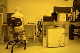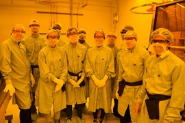
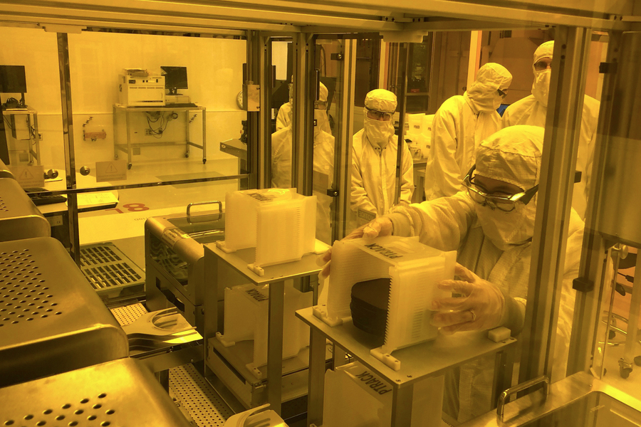
MIT undergraduates are using labs at MIT.nano to tinker at the nanoscale, exploring spectrometry, nanomaterial synthesis, photovoltaics, sensor fabrication, and other topics. They’re also getting an experience not common at the undergraduate level — gowning up in a bunny suit and performing hands-on research inside a clean room.
During the fall 2021 semester, these students were part of 6.S059 (Nanotechnology — Design From Atoms to Everything) and 6.A06 (First.nano! - Fabricate Your Own Solar Cell in MIT.nano Cleanroom), two classes offered by the Department of Electrical Engineering and Computer Science (EECS) aimed at introducing undergraduates to nanoscience through design-focused learning utilizing relevant fabrication processes and tool sets.
“Classes like these can be transformational experiences for our students,” says MIT.nano Director Vladimir Bulović, the Fariborz Maseeh (1990) Chair in Emerging Technology. “They spread the message that nanoscience is at your fingertips. It’s not some far-off, abstract concept, but accessible here and now. We are thrilled to see MIT faculty inspiring and shaping the future leaders of science and technology by showing them what they can master inside MIT.nano.”
Using simple tools to encourage broad exploration
Class 6.S059 was developed to bridge the fundamentals of engineering design with the actual building of functional integrated technologies, something typically separated into multiple classes and semesters.
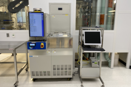
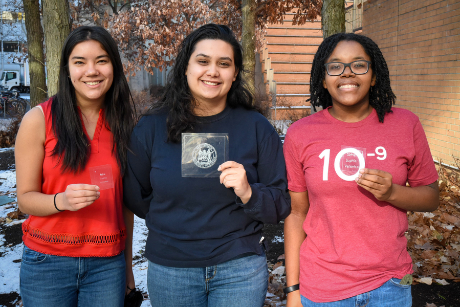
Over nine weeks, 18 students from five different academic departments learned several nanoscale prototyping techniques in MIT.nano including spin coating, maskless lithography, 3D printing, colloidal synthesis, sputtering, evaporation, and optical microscopy. By focusing on a variety of simple tools, the students could do much of the work without needing extensive, specialized training. Rather than watching teaching assistants run equipment, these undergraduates could do the research themselves and, in the process, focus on how the science works, as opposed to how to operate a complicated setup.
“We wanted to teach the science of what you need to design nanodevices and systems in an interactive and hands-on way,” says co-instructor Farnaz Niroui, the EE Landsman (1958) Career Development Assistant Professor of Electrical Engineering and Computer Science at MIT. “Often, these introductory courses take on a heavy mathematical/theoretical approach, which can make it hard to maintain students’ interest. We decided to teach it through an applied approach — having the students design and build, while learning the fundamentals along the way.”
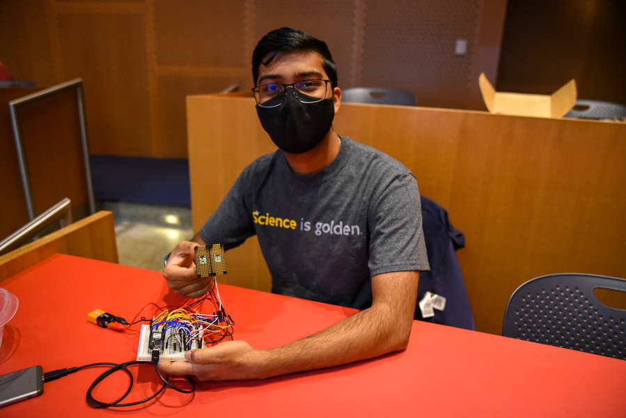
Instead of giving instructions on how to do each step in weekly labs, Niroui and co-instructor Rajeev Ram, professor of electrical engineering, taught the end result (such as using light to observe things you cannot see with the naked eye) and then let the students experiment with assembling the tool set needed to get there (such as designing and building their own microscopes and handheld spectrometers). Each week’s project built on the one before. For example, the undergraduates first designed their own spectrometers, then fabricated the optical grating and a 3D printed case to assemble the tool. This led to a hands-on introduction to CAD design, photolithography, and 3D printing, followed by playing with different light sources and testing their devices on real-world applications by measuring the chlorophyll in a leaf and the emission of quantum dots.
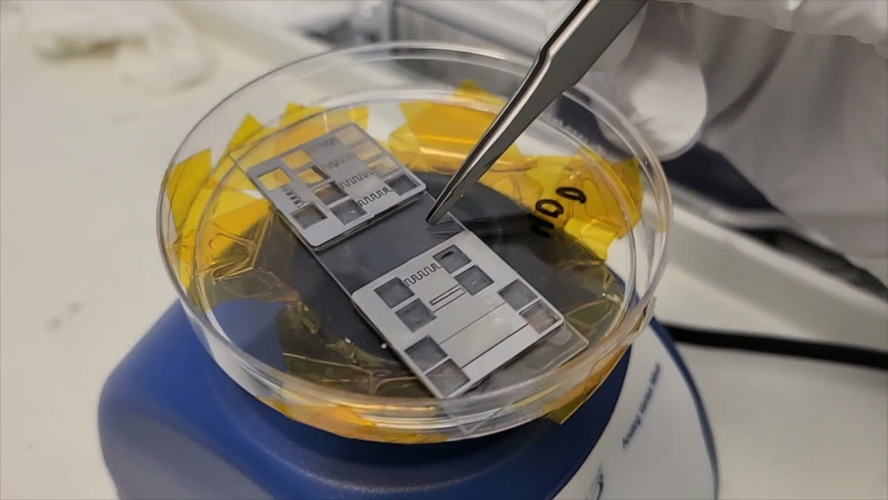
For their final project, the students divided into teams to design and build their own functioning devices. Each project had to use materials and techniques covered in the class, and have at least one feature smaller than 100 nanometers. All six teams were ultimately successful, overcoming challenges to create stretchable sensors using silver nanowires, seven-segment pixelated displays for wearable applications, a programmable organic light-emitting diode matrix, light-trapping microstructures for thin-film solar cells, color-tunable light-emitting diode, and printing fluorescent ink on flexible substrates.
“Seeing the students design and build their own devices after only a few weeks of instruction was exciting and impressive,” says Ram. “It showed that hands-on introduction to advanced concepts in physics can really provide undergraduates with useful, working knowledge about nanotechnology.”
This was the first year for the design-focused nanotechnology class. Niroui and Ram hope to scale it up in future semesters, expanding the offering to more undergraduates.
“Many of the students have said they are excited to explore further into the world of applied science and hardware engineering,” says teaching assistant Mayuran Saravanapavanantham, a PhD candidate in EECS. “One even said they searched MIT’s course listings for anything with the term 'nano'.” Saravanapavanantham was one of three TAs for 6.S059, along with Roberto Brenes and Peter Satterthwaite, all EECS doctoral students.
An early glimpse into the nanoworld
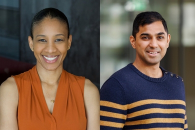
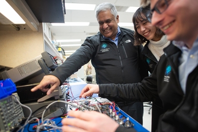
“First.nano!," an advising seminar for first-year students, had similar goals: showing undergraduates what’s possible at the nanoscale through hands-on clean-room experiences. For three hours each week, MIT students in 6.A06 explored MIT.nano’s facilities, experimenting with nanotechnology tool sets and building silicon solar cells under the guidance of co-instructors Jesús del Alamo, the Donner Professor of Engineering, and Jorg Scholvin, the MIT.nano assistant director for user services.
“How do we get first-year students interested in nanofabrication?” asks Jorg Scholvin. “Bring them into the clean room and let them learn by doing things in the lab.” The strategy definitely sparked interest: More than 30 incoming undergraduates applied to fill one of the eight slots offered in the seminar.
Students don’t typically enter the clean room during their undergraduate studies, says Scholvin. By introducing them to nanofabrication in their first semester, del Alamo and Scholvin hope to accelerate their paths into nano-related fields. And, with experience working in a particle-free environment, Scholvin says, these students are now prepared for future opportunities, such as conducting nanoscale research with faculty through the Undergraduate Research Opportunities Program.
“One of the goals of First.nano! was to share our passion for nanofabrication,” says del Alamo. “MIT.nano is an extraordinary facility. By creating opportunities for these students to work and study here, we hope to open it up to broad use for undergraduate research and education.”
Undergraduates from both 6.S059 and 6.A06 are invited to present their work at the Microsystems Annual Research Conference (MARC), co-sponsored by MIT.nano and the Microsystems Technology Laboratories in January. The event, which brings together over 200 students, faculty, and industry partners to celebrate scientific advances in nanotechnology, traditionally features presentations by graduate-level students.