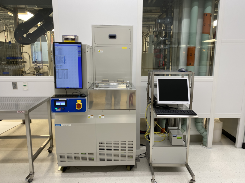
To expand the types of materials that researchers can process, MIT.nano has acquired a new SAMCO inductively coupled plasma (ICP) reactive-ion etching (RIE) system. The instrument has been installed and qualified on the third floor of MIT.nano, where it is now available for training and use.
Reactive-ion etching is a material removal process performed under low pressure in which a reactive plasma is generated to remove the material on the substrate. With inductively coupled plasma RIE, the plasma is generated by a radio-frequency-powered magnetic field to ionize different gases.
The etching of different materials is determined by the type and amount of the gas, with any volatile byproducts removed in the effluent. The SAMCO RIE-230iP ICP etcher combines fluorine, chlorine, and bromine chemistries from 11 different process gases to provide broad etching capabilities for a wide variety of novel materials and materials research. The tool has a load-lock system, which allows the reaction chamber to stay under vacuum when loading and unloading substrates. The controlled environment improves process repeatability and throughput, as well as increases safety when using corrosive gases.
“The new SAMCO etcher’s ability to handle a range of materials gives researchers more flexibility in the choice of substrates and films for their devices,” says Jorg Scholvin, assistant director of user services at Fab.nano. “It will significantly expand the process capabilities available at MIT.nano, particularly when exploring new types of materials and devices.”
The SAMCO RIE etcher adds two new etch chemistries — hydrogen bromide and nitrogen trifluoride — in addition to enabling the mixing of chemistries. It can process samples as small as a few millimeters, or wafers up to 8 inches in diameter. Nitrogen trifluoride was added for improved chamber cleaning between etch chemistries and different substrate materials.
Another feature of this tool is the integrated optical endpoint spectrometer (OES), which monitors the plasma and gas effluence, letting the researcher know when etching is complete. The OES does this by looking at etched material in the optical spectrum; when the signal disappears, all the material has been etched away. The new tool also has a circulator that allows for substrate temperature control from 20 degrees Celsius up to 200 C. This is important because some etch byproducts are not sufficiently volatile unless heated to a high temperature.
The new instrument was purchased with Lord Foundation of Massachusetts funding secured by the Department of Materials Science and Engineering.
SAMCO is a semiconductor and materials company focused on material processing and device manufacturing. The SAMCO RIE-230iP etcher adds to MIT.nano’s suite of existing SAMCO tools, which include a fluorine-chemistry etcher, a chlorine-chemistry etcher, and a plasma-enhanced chemical vapor deposition tool for thin film deposition.
For more information about MIT.nano’s tools and instruments, visit nanousers.mit.edu.
