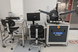
MIT.nano has acquired a Raith VELION focused ion beam scanning electron microscope (FIB-SEM) as a demonstration unit in its characterization facility. The instrument, which arrived on campus last summer, has been installed and qualified in the lower level of Building 12 and is now available for training and use.
The VELION will augment the MIT.nano fabrication and characterization tool sets and enable next-generation nanofabrication by providing users with the capability to fabricate two- and three-dimensional nanostructures with high resolution over large areas, explains Anna Osherov, assistant director for user services at Characterization.nano. The tool will also facilitate new studies of electrical transport and surface modification with novel three-dimensional geometries.
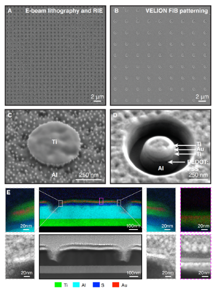
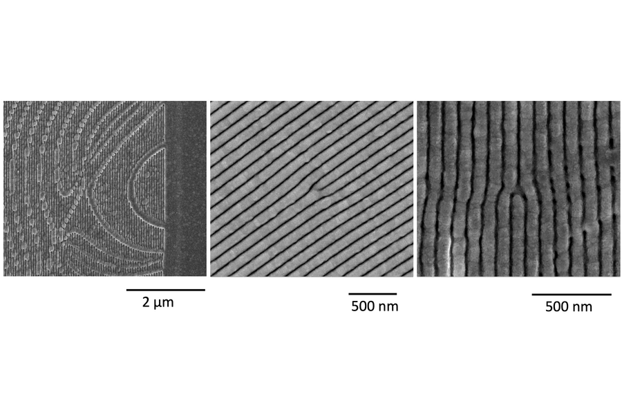
The VELION offers capabilities for advanced focused ion beam nanofabrication while also allowing versatile sample preparation, process control, and entry-level e-beam lithography — all in one tool. The unit comprises a top-down mounted multi-ion milling species nanoFIB column perpendicular to a laser interferometer stage with an attached field emission scanning electron microscope column. This unique setup enables high-precision patterning resolution as well as unprecedented process stability, accuracy, and automation.
The VELION provides a single-step automated substitute for multi-step conventional nanofabrication processing that usually involves e-beam lithography and multiple reactive ion etching steps. Osherov says, “This tool offers researchers using our facilities the potential for a substantial reduction in both overall processing time and human effort.”
Conventional dual-beam instruments — with a scanning electron microscope plus focused ion beam — typically lack the patterning resolution and stability that is essential for plasmonic devices, metamaterials, nanofluidics, waveguides, Fresnel lenses, nanophotonics, and quantum devices. In contrast, the VELION combines the strength of precise large-area patterning while maintaining high resolution with the focused ion source. This combination enables processing and patterning of materials that are otherwise difficult to explore with conventional lithographic approaches.
To achieve performance stability, essential for automated nanofabrication, it was imperative that the VELION be placed in a location optimized for low vibration and low electromagnetic interference. According to representatives from Raith, the VELION installed in MIT.nano’s basement imaging suite has demonstrated record performance stability that can be attributed to the combination of the stability-oriented design of the VELION nanofabrication system and exceptional engineering controls of the MIT.nano space. The average beam position drift of less than 5 nanometers per hour over the 16-hour measurement period is a performance not previously achieved on the VELION.
To enable chemical modification in conjunction with patterning, the VELION is equipped with multiple ion sources for processing, including gold, germanium, and silicon. This provides flexibility in implantation and contact patterning where the Silicon++ ion source achieves beam diameter well below 8 nm and the carbon and platinum gas injection system achieves 50 nm patterning. In combination with sub-A pitch control of the grating and near-zero stitching error, it is possible to both fabricate nanostructures and deposit electrical contacts in one consecutive process in the same system.
More than 25 individual projects — ranging from diamond photonics to human-machine symbiosis — have already made use of the VELION over the past six months, according to Osherov. The instrument has been made available to the campus as a demonstration unit by Raith, the manufacturer of the VELION and a founding member of the MIT.nano Consortium. The tool is staffed by Raith application scientist Yang Yu who is available to support research activities and join in technical collaboration with MIT researchers.
For more information about the VELION, other MIT.nano tools and instruments, and how to receive access and training, visit nanousers.mit.edu.