Fluorescent nanosensor enables rapid, first-of-its-kind detection of key gut health biomarker
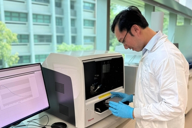
Researchers developed an optical nanosensor to rapidly detect a key gut biomarker, enabling faster, accessible screening.
Researchers developed an optical nanosensor to rapidly detect a key gut biomarker, enabling faster, accessible screening.
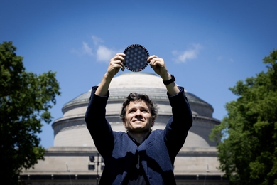
The MIT physicist shares the honor with two others for foundational research establishing the field of twistronics.

By using a thin layer of diamond to manage excessive heat, researchers can boost the speed and energy-efficiency of next-generation wireless devices.
The adjuvant can help the injectable polio vaccine induce a strong immune response in the GI tract, which is considered critical to eradicating the virus.
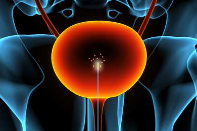
Using a catheter coated with carbon nanotubes, researchers can detect biomarkers produced by cancer cells in the bladder.
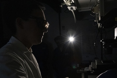
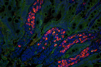
Researchers can now use custom-built microscopy and nanotechnology to tag and follow the activity of individual proteins in real-time.
The MIT Marble Center for Cancer Nanomedicine looks back at 10 years of turning big ideas about nanotechnology into transformative advances for cancer patients.

The discovery of dioxaborirane could expand the chemistry of boron-based reagents, providing new tools for oxidation reactions in synthesis and materials science.

A new method for precisely moving columns of individual atoms within a material could give rise to exotic quantum properties.
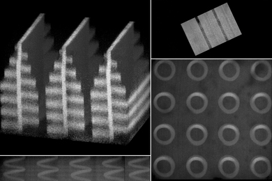
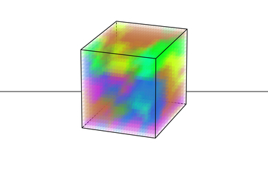
MIT researchers created tiny 3D photonic devices with features small enough to channel visible light.
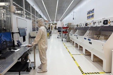
NanoFab Equipment Management and Operations (NEMO) system streamlines shared facilities management via tool trainings, reservations, and lab communications.
Relaxor ferroelectrics have been used in electronics and sensors for decades, but the source of their unique properties was a mystery until now.
Startup accelerator program grows to over 30 companies, almost half of them with MIT pedigrees.

The electrical engineering and nanotechnology leader will guide the US Army-sponsored research center as it advances next-generation materials, electronics, and photonics for national security.