Nanostructures are a stunning array of intricate patterns that are imperceptible to the human eye, yet they help power modern life. They are the building blocks of microchip transistors, etched onto grating substrates of space-based X-ray telescopes, and drive innovations in medicine, sustainability, and quantum computing.
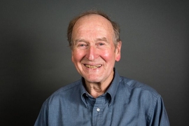
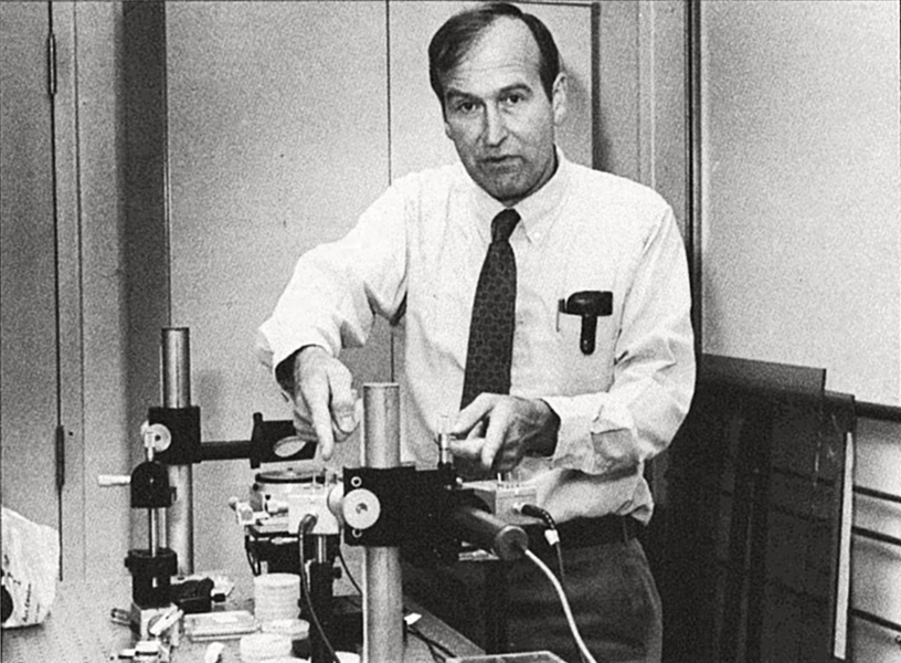
Since the 1970s, Henry “Hank” Smith, MIT professor emeritus of electrical engineering, has been a leading force in this field. He pioneered the use of proximity X-ray lithography, proving that X-rays’ short optical wavelength could produce high-resolution patterns at the nanometer scale. Smith also made significant advancements in phase-shifting masks (PSMs), a technique that disrupts light waves to enhance contrast. His design of attenuated PSMs, which he co-created with graduate students Mark Schattenburg PhD ʼ84 and Erik H. Anderson ʼ81, SM ʼ84, PhD ʼ88, is still used today in the semiconductor industry.
In recognition of these contributions, as well as highly influential achievements in liquid-immersion lithography, achromatic-interference lithography, and zone-plate array lithography, Smith recently received the 2025 SPIE Frits Zernike Award for Microlithography. Given by the Society of Photo-Optical Instrumentation Engineers (SPIE), the accolade recognizes scientists for their outstanding accomplishments in microlithographic technology.
“The Zernike Award is an impressive honor that aptly recognizes Hank’s pioneering contributions,” says Karl Berggren, MIT’s Joseph F. and Nancy P. Keithley Professor in Electrical Engineering and faculty head of electrical engineering. “Whether it was in the classroom, at a research conference, or in the lab, Hank approached his work with a high level of scientific rigor that helped make him decades ahead of industry practices.”
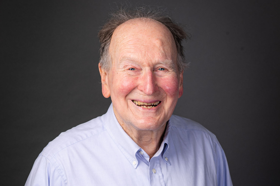
Now 88 years old, Smith has garnered many other honors. He was also awarded the SPIE BACUS Prize, named a member of the National Academy of Engineering, and is a fellow of the American Academy of Arts and Sciences, IEEE, the National Academy of Inventors, and the International Society for Nanomanufacturing.
Jump-starting the nano frontier
From an early age, Smith was fascinated by the world around him. He took apart clocks to see how they worked, explored the outdoors, and even observed the movement of water. After graduating from high school in New Jersey, Smith majored in physics at College of the Holy Cross. From there, he pursued his doctorate at Boston College and served three years as an officer in the U.S. Air Force.
It was his job at MIT Lincoln Laboratory that ultimately changed Smith’s career trajectory. There, he met visitors from MIT and Harvard University who shared their big ideas for electronic and surface acoustic wave devices but were stymied by the physical limitations of fabrication. Yet, few were inclined to tackle this challenge.
“The job of making things was usually brushed off the table with, ‘oh well, we’ll get some technicians to do that,’” Smith said in his oral history for the Center for Nanotechnology in Society. “And the intellectual content of fabrication technology was not appreciated by people who had been ‘traditionally educated,’ I guess.”
More interested in solving problems than maintaining academic rank, Smith set out to understand the science of fabrication. His breakthrough in X-ray lithography signaled to the world the potential and possibilities of working on the nanometer scale, says Schattenburg, who is a senior research scientist at MIT Kavli Institute for Astrophysics and Space Research.
“His early work proved to people at MIT and researchers across the country that nanofabrication had some merit,” Schattenburg says. “By showing what was possible, Hank really jump-started the nano frontier.”
Cracking open lithography’s black box
By 1980, Smith left Lincoln Lab for MIT’s main campus and continued to push forward new ideas in his NanoStructures Laboratory (NSL), formerly the Submicron Structures Laboratory. NSL served as both a research lab and a service shop that provided optical gratings, which are pieces of glass engraved with sub-micron periodic patterns, to the MIT community and outside scientists. It was a busy time for the lab; NSL attracted graduate students and international visitors. Still, Smith and his staff ensured that anyone visiting NSL would also receive a primer on nanotechnology.
“Hank never wanted anything we produced to be treated as a black box,” says Mark Mondol, MIT.nano e-beam lithography domain expert who spent 23 years working with Smith in NSL. “Hank was always very keen on people understanding our work and how it happens, and he was the perfect person to explain it because he talked in very clear and basic terms.”
The physical NSL space in MIT Building 39 shuttered in 2023, a decade after Smith became an emeritus faculty member. NSL’s knowledgeable staff and unique capabilities transferred to MIT.nano, which now serves as MIT’s central hub for supporting nanoscience and nanotechnology advancements. Unstoppable, Smith continues to contribute his wisdom to the ever-expanding nano community by giving talks at the NSL Community Meetings at MIT.nano focused on lithography, nanofabrication, and their future.
Smith’s career is far from complete. Through his startup LumArray, Smith continues to push the boundaries of knowledge. He recently devised a maskless lithography method, known as X-ray Maskless Lithography (XML), that has the potential to lower manufacturing costs of microchips and thwart the sale of counterfeit microchips.
Dimitri Antoniadis, MIT professor emeritus of electrical engineering and computer science, is Smith’s longtime collaborator and friend. According to him, Smith’s commitment to research is practically unheard-of.
“Once professors reach emeritus status, we usually inspire and supervise research,” Antoniadis says. “It’s very rare for retired professors to do all the work themselves, but he loves it.”
Enduring influence
Smith’s legacy extends far beyond the groundbreaking tools and techniques he pioneered, say his friends, colleagues, and former students. His relentless curiosity and commitment to his graduate students helped propel his field forward.
He earned a reputation for sitting in the front row at research conferences, ready to ask the first question. Fellow researchers sometimes dreaded seeing him there.
“Hank kept us honest,” Berggren says. “Scientists and engineers knew that they couldn’t make a claim that was a little too strong, or use data that didn’t support the hypothesis, because Hank would hold them accountable.”
Smith never saw himself as playing the good cop or bad cop — he was simply a curious learner unafraid to look foolish.
“There are famous people, Nobel Prize winners, that will sit through research presentations and not have a clue as to what’s going on,” Smith says. “That is an utter waste of time. If I don’t understand something, I’m going to ask a question.”
As an advisor, Smith held his graduate students to high standards. If they came unprepared or lacked understanding of their research, he would challenge them with tough, unrelenting questions. Yet, he was also their biggest advocate, helping students such as Lisa Su SB/SM ʼ91, PhD ʼ94, who is now the chair and chief executive officer of AMD, and Dario Gil PhD ʼ03, who is now the chair of the National Science Board and senior vice president and director of research at IBM, succeed in the lab and beyond.
Research Specialist James Daley has spent nearly three decades at MIT, most of them working with Smith. In that time, he has seen hundreds of advisees graduate and return to offer their thanks. “Hank’s former students are all over the world,” Daley says. “Many are now professors mentoring their own graduate students and bringing with them some of Hank’s style. They are his greatest legacy.”