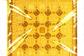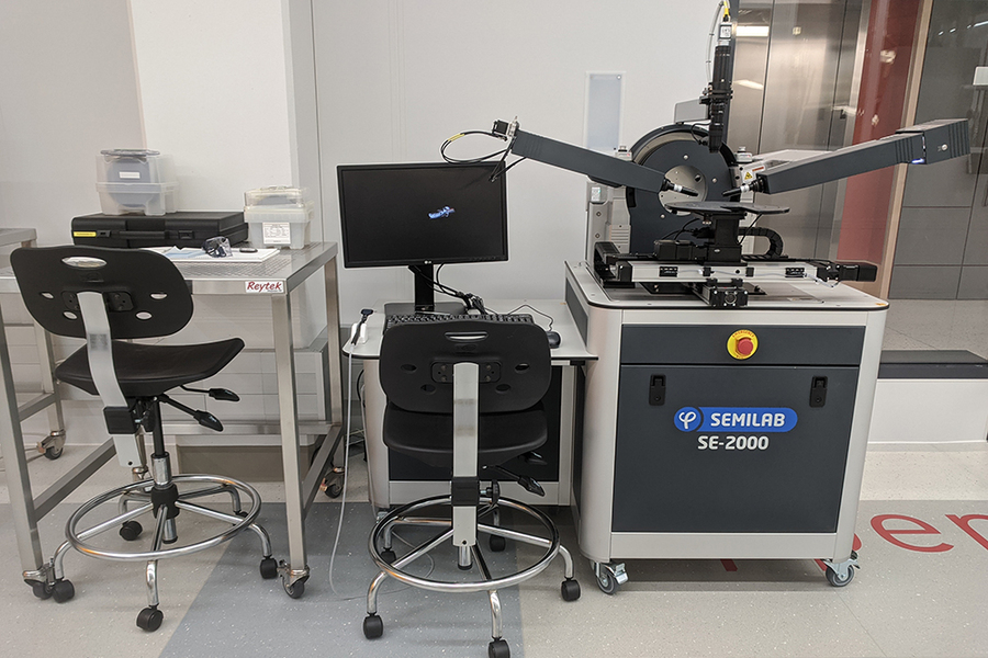
In nanofabrication, it is important to characterize and understand the physical, mechanical, and chemical properties of the various thin-film materials used to build devices. Ellipsometry is a particularly valuable technique for non-destructive optical characterization of a wide variety of thin-film materials — such as semiconductors, dielectrics, polymers, and metals — as well as complex multilayered structures. By measuring the change in the light polarization upon interaction with the matter, information such as thickness, refractive index, dielectric permittivity, composition, and doping can be revealed.
To expand thin-film measurement capabilities available to its researchers, MIT.nano recently acquired a Semilab SE-2000 Spectroscopic Ellipsometer. The instrument has been installed and qualified in the third-floor clean room in Building 12, and is now available for training and use.
The Semilab ellipsometer will augment the MIT.nano clean room metrology capabilities by addressing the need for a broad spectral range (from 245 nm–1,700 nm), autofocus, automatic goniometer for incidence angle adjustment (20-90 degrees), and large-area (300 mm) automatic stage with mapping capabilities, according to Anna Osherov, assistant director of user services for Characterization.nano.
“We’re delighted to add this tool to the growing set of instruments and equipment available to MIT.nano users,” she says. “We’re developing a powerful set of ex-situ and in-situ capabilities for characterization and metrology in our facilities, and ellipsometry is yet another fundamental technique that will advance research for many users.”
With Microspot optics and an optical camera for region-of-interest visualization, the instrument is able to uniformly assess samples ranging from pieces up to 300 mm wafers. The SE-2000 replaces the capabilities that had been provided by the decommissioned Tencor UV1280, which was located in the second-floor Integrated Circuits Laboratory in Building 39.
Semilab designs and manufactures metrology equipment for the characterization of semiconductor and photovoltaic materials, and for the R&D and manufacturing processes of semiconductor devices, flat-panel displays, and solar cells.
For more information about MIT.nano’s tools and instruments, visit nanousers.mit.edu.