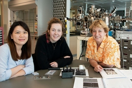

Though Frances Ross and her sister Caroline Ross both ended up on the faculty of MIT’s Department of Materials Science and Engineering, they got there by quite different pathways. While Caroline followed a more traditional academic route and has spent most of her career at MIT, Frances Ross spent most of her professional life working in the industrial sector, as a microscopy specialist at IBM. It wasn’t until 2018 that she arrived at MIT to oversee the new state-of-the-art electron microscope systems being installed in the new MIT.nano facility.
Frances, who bears a strong family resemblance to her sister, says “it’s confused a few people, if they don’t know there are two of us.”
The sisters grew up in London in a strongly science- and materials-oriented family. Her father, who worked first as a scientist and then as a lawyer, is currently working on his third PhD degree, in classics. Her mother, a gemologist, specializes in precisely matching diamonds, and oversees certification testing for the profession.
After earning her doctorate at Cambridge University in materials science, specializing in electron microscopy, Frances Ross went on to do a postdoc at Bell Labs in New Jersey, and then to the National Center for Electron Microscopy at the University of California at Berkeley. From there she continued her work in electron microscopy at IBM in Yorktown Heights, New York, where she spent 20 years working on development and application of electron microscope technology to studying crystal growth.
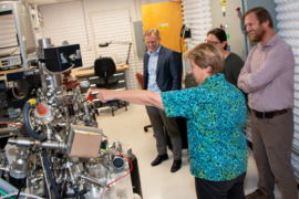
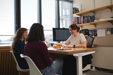
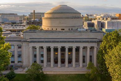
When MIT built its new cutting-edge nanotechnology fabrication and analysis facility, MIT.nano, it was clear that state-of-the-art microscope technology would need to be a key feature of the new center. That’s when Ross was hired as a professor, along with Professor Jim LeBeau and Research Scientist Rami Dana, who had an academic and industrial research background, to oversee the creation, development, and application of those microscopes for the Department of Materials Science and Engineering (DMSE) and the wider MIT community.
“Currently, our students have to go to other places to do high-performance microscopy, so they might go to Harvard, or one of the national labs,” says Ross, who is the Ellen Swallow Richards Professor in Materials Science and Engineering. “Very many advances in the instrumentation have come together over the last few years, so that if your equipment is a little older, it’s actually a big disadvantage in electron microcopy. This is an area where MIT had not invested for a little while, and therefore, once they made that decision, the jump is going to be very significant. We’re going to have a state-of-the-art imaging capability.”
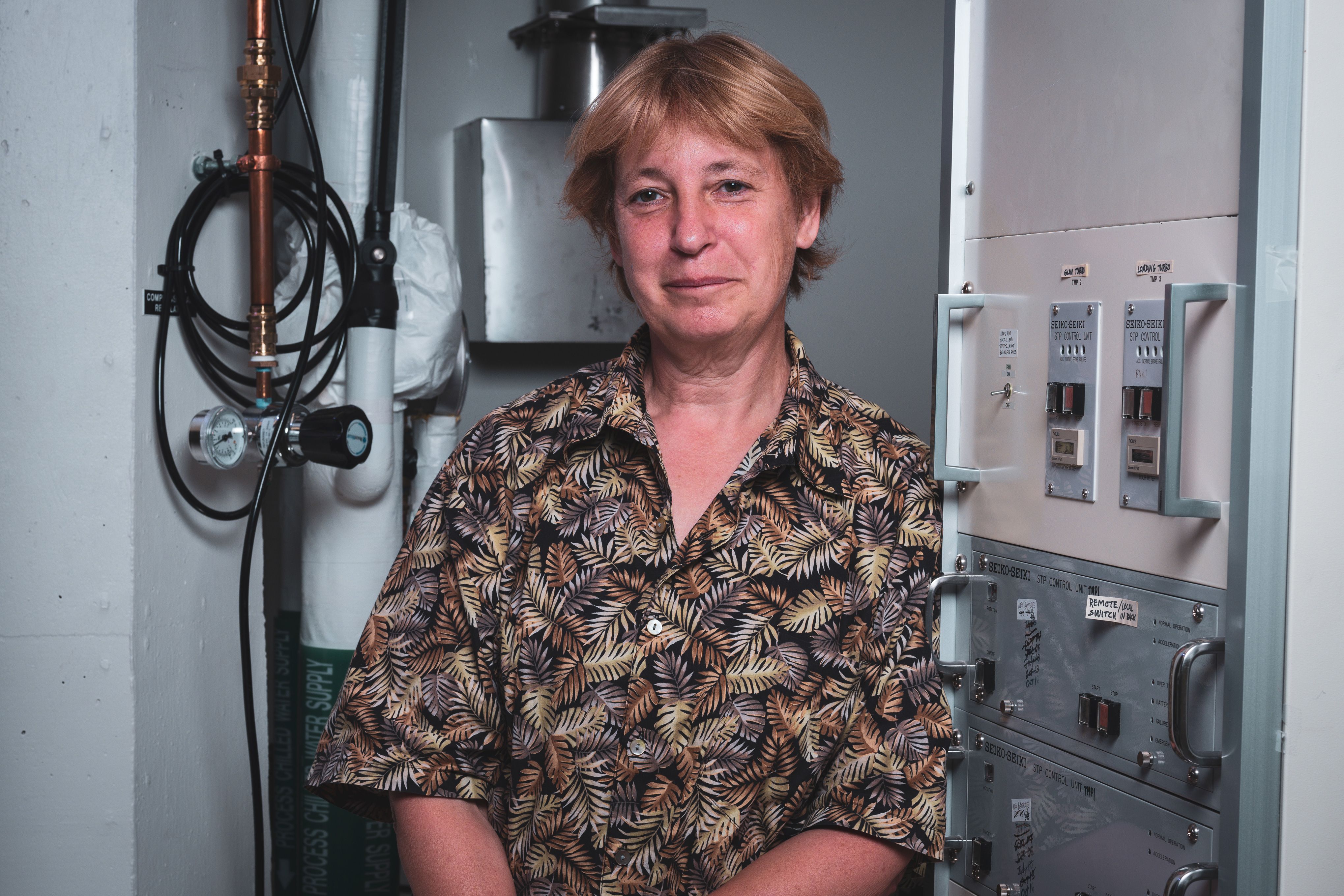
There will be two major electron microscope systems for materials science, which are gradually taking shape inside the vibration-isolated basement level of MIT.nano, alongside two others already installed that are specialized for biomedical imaging.
One of these will be an advanced version of a standard electron microscope, she says, that will have a unique combination of features. “There is nothing that exists with the capabilities that we are aiming for here.”
The most important of these, she says, is the quality of the vacuum inside the microscope: “In most of our experiments, we want to start with a surface that’s atomically clean.” For example, “we could start with atomically clean silicon, and then add some germanium. How do the germanium atoms add onto the silicon surface? That’s a very important question for microelectronics. But if the sample is in an environment that’s not well-controlled, then the results you get will depend on how dirty the vacuum is. Contamination may affect the process, and you can’t be sure that what you’re seeing is what happens in real life.” Ross is working with the manufacturers to reach exceptional levels of cleanliness in the vacuum of the electron microscope system being developed now.
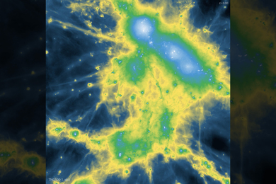
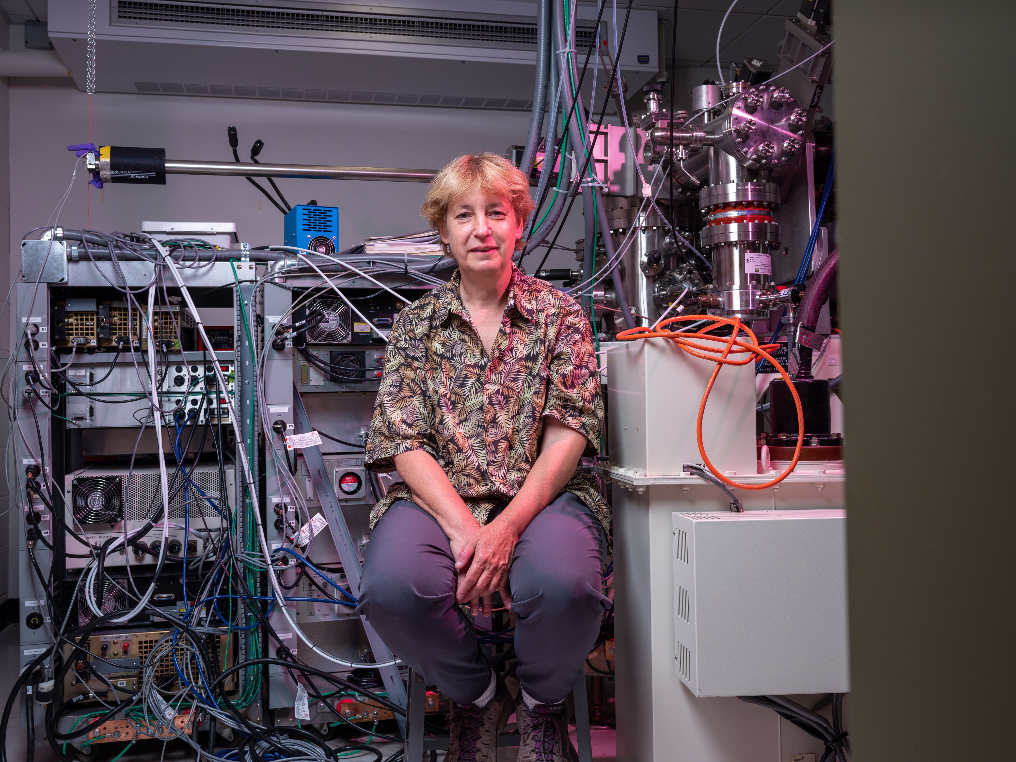
But ultra-high-quality vacuum is just one of its attributes. “We combine the good vacuum with capabilities to heat the sample, and flow gases, and record images at high speed,” Ross says. “Perhaps most importantly for a lot of our experiments, we use lower-energy electrons to do the imaging, because for many interesting materials like 2D materials, such as graphene, boron nitride, and related structures, the high-energy electrons that are normally used will damage the sample.”
Putting that all together, she says, “is a unique instrument that will give us real insights into surface reactions, crystal growth processes, materials transformations, catalysis, all kinds of reactions involving nanostructure formation and chemistry on the surfaces of 2D materials.”
Other instruments and capabilities are also being added to MIT’s microscopy portfolio. A new scanning transmission electron microscope is already installed in MIT.nano and is providing high-resolution structural and chemical analysis of samples for several projects at MIT. Another new capability is a special sample holder that allows researchers to make movies of unfolding processes in water or other liquids in the microscope. This allows detailed monitoring, at up to 100 frames per second, of a variety of phenomena, such as solution-phase growth, unfolding chemical reactions, or electrochemical processes such as battery charging and discharging. Making movies of processes taking place in water, she says, “is something of a new field for electron microscopy.”
Ross already has set up an ultra-high vacuum electron microscope in DMSE but without the resolution and low-voltage operation of the new instrument. And finally, an ultra-high vacuum scanning tunneling microscope has just started to produce images and will measure current flow through nanoscale materials.
In their free time, Ross and her husband Brian enjoy sailing, mostly off the coast of Maine, with their two children, Kathryn and Eric. As a hobby she collects samples of beach sand. “I have a thousand different kinds of sand from various places, and a lot of them from Massachusetts,” she says. “Everywhere I go, that’s my souvenir.”
But with her intense focus on developing this new world-class microscopy facility, there’s little time for anything else these days. Her aim is to ensure that it’s the best facility possible.
“I’m hoping that MIT becomes a center for electron microscopy,” she says. “You know, with all the interesting materials science and physics that goes on here, it matches up very well with this unique instrumentation, this high-quality combination of imaging and analysis. These unique characterization capabilities really complement the rest of the science that happens here.”