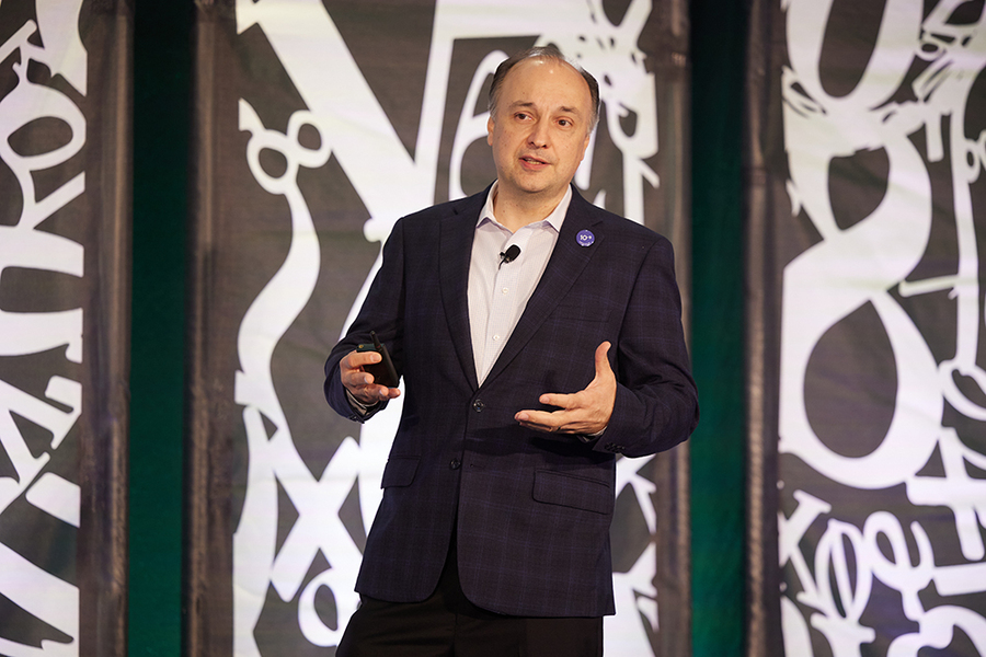
There is vast opportunity for nanoscale innovation to transform the world in positive ways — expressed MIT.nano Director Vladimir Bulović as he posed two questions to attendees at the start of the inaugural Nano Summit: “Where are we heading? And what is the next big thing we can develop?”
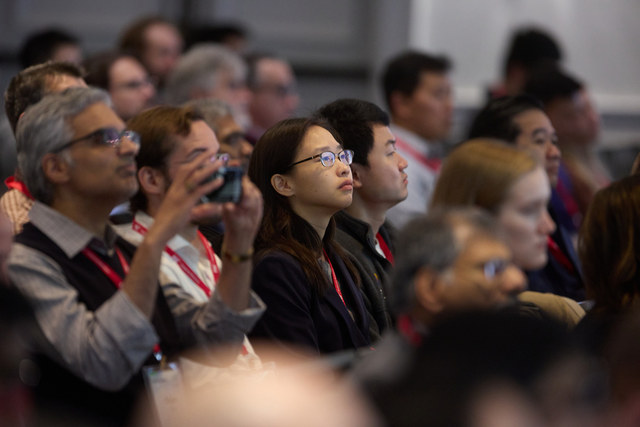
“The answer to that puts into perspective our main purpose — and that is to change the world,” Bulović, the Fariborz Maseeh Professor of Emerging Technologies, told an audience of more than 325 in-person and 150 virtual participants gathered for an exploration of nano-related research at MIT and a celebration of MIT.nano’s fifth anniversary.
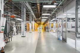
Over a decade ago, MIT embarked on a massive project for the ultra-small — building an advanced facility to support research at the nanoscale. Construction of MIT.nano in the heart of MIT’s campus, a process compared to assembling a ship in a bottle, began in 2015, and the facility launched in October 2018.
Fast forward five years: MIT.nano now contains nearly 170 tools and instruments serving more than 1,200 trained researchers. These individuals come from over 300 principal investigator labs, representing more than 50 MIT departments, labs, and centers. The facility also serves external users from industry, other academic institutions, and over 130 startup and multinational companies. And in 2022, MIT.nano's home — Building 12 — was named in honor of Lisa T. Su ’90, SM ’91, PhD ’94, chief executive officer and chair of the Board of Directors of AMD.
A cross section of these faculty and researchers joined industry partners and MIT community members to kick off the first Nano Summit, which is expected to become an annual flagship event for MIT.nano and its industry consortium. Held on Oct. 24, the inaugural conference was co-hosted by the MIT Industrial Liaison Program.
Six topical sessions highlighted recent developments in quantum science and engineering, materials, advanced electronics, energy, biology, and immersive data technology. The Nano Summit also featured startup ventures and an art exhibition.
Seeing and manipulating at the nanoscale — and beyond
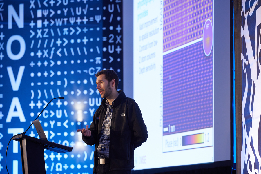
“We need to develop new ways of building the next generation of materials,” said Frances Ross, the TDK Professor in Materials Science and Engineering (DMSE). “We need to use electron microscopy to help us understand not only what the structure is after it’s built, but how it came to be. I think the next few years in this piece of the nano realm are going to be really amazing.”
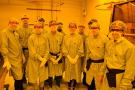
Speakers in the session “The Next Materials Revolution,” chaired by MIT.nano co-director for Characterization.nano and associate professor in DMSE James LeBeau, highlighted areas in which cutting-edge microscopy provides insights into the behavior of functional materials at the nanoscale, from anti-ferroelectrics to thin-film photovoltaics and 2D materials. They shared images and videos collected using the instruments in MIT.nano’s characterization suites, which were specifically designed and constructed to minimize mechanical-vibrational and electro-magnetic interference.
Later, in the “Biology and Human Health” session chaired by Boris Magasanik Professor of Biology Thomas Schwartz, biologists echoed the materials scientists, stressing the importance of the ultra-quiet, low-vibration environment in Characterization.nano to obtain high-resolution images of biological structures.
“Why is MIT.nano important for us?” asked Schwartz. “An important element of biology is to understand the structure of biology macromolecules. We want to get to an atomic resolution of these structures. CryoEM (cryo-electron microscopy) is an excellent method for this. In order to enable the resolution revolution, we had to get these instruments to MIT. For that, MIT.nano was fantastic.”
Seychelle Vos, the Robert A. Swanson (1969) Career Development Professor of Life Sciences, shared CryoEM images from her lab’s work, followed by biology Associate Professor Joey Davis who spoke about image processing. When asked about the next stage for CryoEM, Davis said he’s most excited about in-situ tomography, noting that there are new instruments being designed that will improve the current labor-intensive process.
To chart the future of energy, chemistry associate professor Yogi Surendranath is also using MIT.nano to see what is happening at the nanoscale in his research to use renewable electricity to change carbon dioxide into fuel.
“MIT.nano has played an immense role, not only in facilitating our ability to make nanostructures, but also to understand nanostructures through advanced imaging capabilities,” said Surendranath. “I see a lot of the future of MIT.nano around the question of how nanostructures evolve and change under the conditions that are relevant to their function. The tools at MIT.nano can help us sort that out.”
Tech transfer and quantum computing
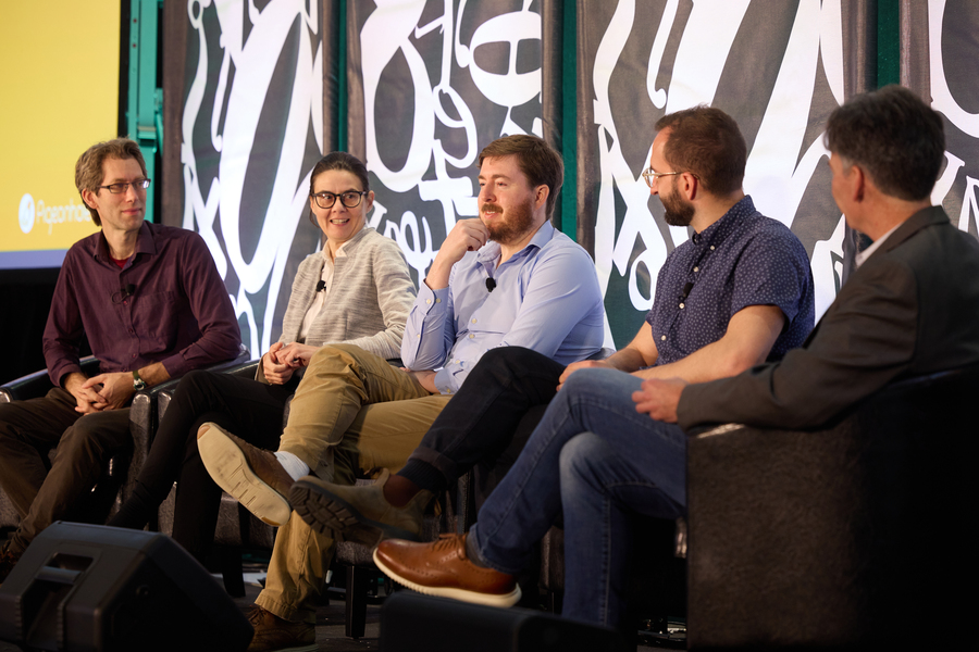
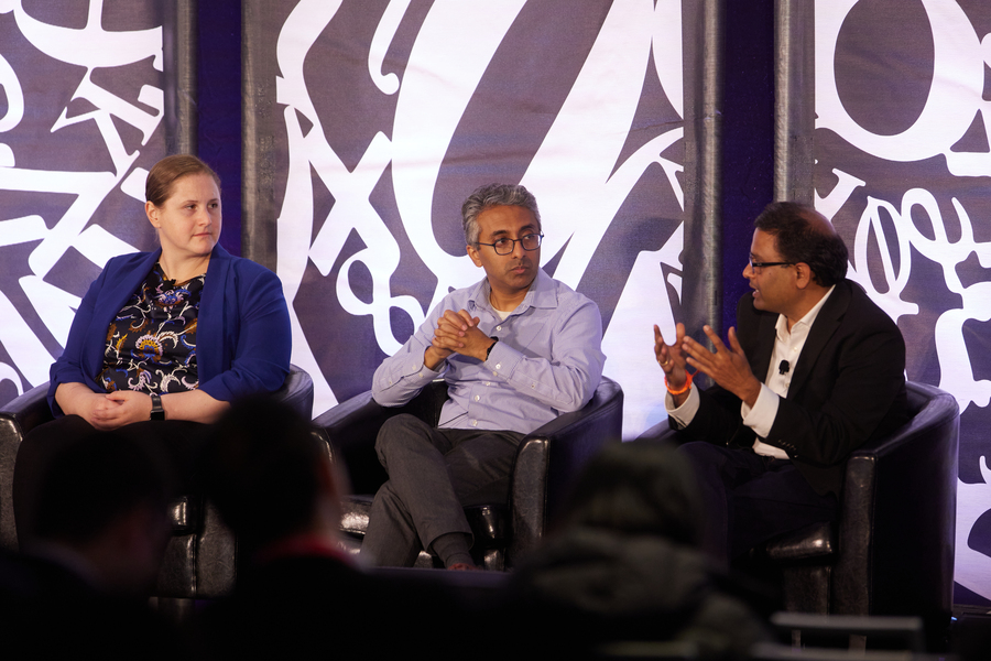
The “Advanced Electronics” session chaired by Jesús del Alamo, the Donner Professor of Science in the Department of Electrical Engineering and Computer Science (EECS), brought together industry partners and MIT faculty for a panel discussion on the future of semiconductors and microelectronics. “Excellence in innovation is not enough, we also need to be excellent in transferring these to the marketplace,” said del Alamo. On this point, panelists spoke about strengthening the industry-university connection, as well as the importance of collaborative research environments and of access to advanced facilities, such as MIT.nano, for these environments to thrive.
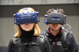
The session came on the heels of a startup exhibit in which eleven START.nano companies presented their technologies in health, energy, climate, and virtual reality, among other topics. START.nano, MIT.nano’s hard-tech accelerator, provides participants use of MIT.nano’s facilities at a discounted rate and access to MIT’s startup ecosystem. The program aims to ease hard-tech startups’ transition from the lab to the marketplace, surviving common “valleys of death” as they move from idea to prototype to scaling up.
When asked about the state of quantum computing in the “Quantum Science and Engineering” session, physics professor Aram Harrow related his response to these startup challenges. “There are quite a few valleys to cross — there are the technical valleys, and then also the commercial valleys.” He spoke about scaling superconducting qubits and qubits made of suspended trapped ions, and the need for more scalable architectures, which we have the ingredients for, he said, but putting everything together is quite challenging.
Throughout the session, William Oliver, professor of physics and the Henry Ellis Warren (1894) Professor of Electrical Engineering and Computer Science, asked the panelists how MIT.nano can address challenges in assembly and scalability in quantum science.
“To harness the power of students to innovate, you really need to allow them to get their hands dirty, try new things, try all their crazy ideas, before this goes into a foundry-level process,” responded Kevin O’Brien, associate professor in EECS. “That’s what my group has been working on at MIT.nano, building these superconducting quantum processors using the state-of-the art fabrication techniques in MIT.nano.”
Connecting the digital to the physical
In his reflections on the semiconductor industry, Douglas Carlson, senior vice president for technology at MACOM, stressed connecting the digital world to real-world application. Later, in the “Immersive Data Technology” session, MIT.nano associate director Brian Anthony explained how, at the MIT.nano Immersion Lab, researchers are doing just that.
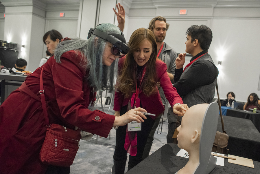
“We think about and facilitate work that has the human immersed between hardware, data, and experience,” said Anthony, principal research scientist in mechanical engineering. He spoke about using the capabilities of the Immersion Lab to apply immersive technologies to different areas — health, sports, performance, manufacturing, and education, among others. Speakers in this session gave specific examples in hardware, pediatric health, and opera.
Anthony connected this third pillar of MIT.nano to the fab and characterization facilities, highlighting how the Immersion Lab supports work conducted in other parts of the building. The Immersion Lab’s strength, he said, is taking novel work being developed inside MIT.nano and bringing it up to the human scale to think about applications and uses.
Artworks that are scientifically inspired
The Nano Summit closed with a reception at MIT.nano where guests could explore the facility and gaze through the cleanroom windows, where users were actively conducting research. Attendees were encouraged to visit an exhibition on MIT.nano’s first- and second-floor galleries featuring work by students from the MIT Program in Art, Culture, and Technology (ACT) who were invited to utilize MIT.nano’s tool sets and environments as inspiration for art.
In his closing remarks, Bulović reflected on the community of people who keep MIT.nano running and who are using the tools to advance their research. “Today we are celebrating the facility and all the work that has been done over the last five years to bring it to where it is today. It is there to function not just as a space, but as an essential part of MIT’s mission in research, innovation, and education. I hope that all of us here today take away a deep appreciation and admiration for those who are leading the journey into the nano age.”