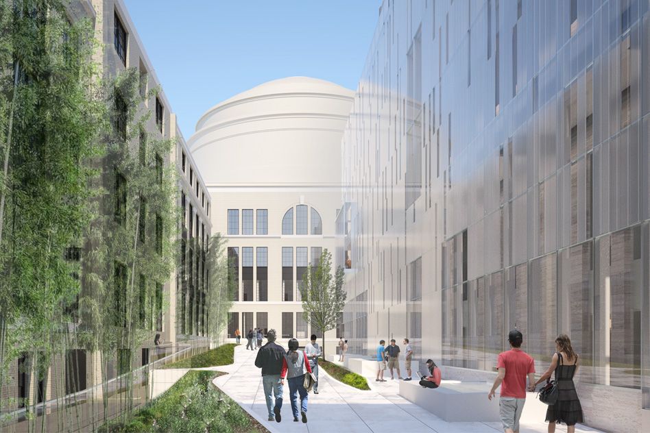


Starting in 2018, researchers from across MIT will be able to take advantage of comprehensive facilities for nanoscale research in a new building to be constructed at the very heart of the Cambridge campus.
The 200,000-square-foot building, called “MIT.nano,” will house state-of-the-art cleanroom, imaging, and prototyping facilities supporting research with nanoscale materials and processes — in fields including energy, health, life sciences, quantum sciences, electronics, and manufacturing. An estimated 2,000 MIT researchers may ultimately make use of the building, says electrical engineering professor Vladimir Bulović, faculty lead on the MIT.nano project and associate dean for innovation in the School of Engineering.
“MIT.nano will sit at the heart of our campus, and it will be central to fulfilling MIT’s mission in research, education, and impact,” says MIT President L. Rafael Reif. “The capabilities it provides and the interdisciplinary community it inspires will keep MIT at the forefront of discovery and innovation, and give us the power to solve urgent global challenges. By following the lead of faculty and student interest, MIT has a long tradition of placing bold bets on strategic future technologies, and we expect MIT.nano to pay off in the same way, for MIT and for the world.”
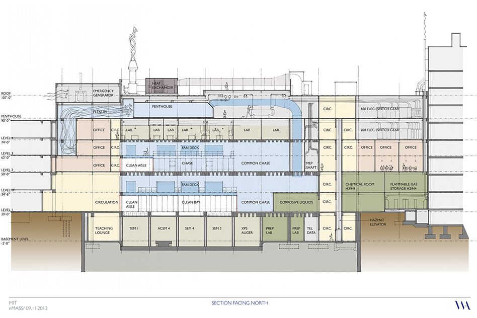
MIT.nano will house two interconnected floors of cleanroom laboratories containing fabrication spaces and materials growth laboratories, greatly expanding the Institute’s capacity for research involving components that are measured in billionths of a meter — a scale at which cleanliness is paramount, as even a single speck of dust vastly exceeds the nanoscale. The building will also include the “quietest” space on campus — a floor optimized for low vibration and minimal electromagnetic interference, dedicated to advanced imaging technologies — and a floor of teaching laboratory space. Finally, the facility will feature an innovative teaching and research space, known as a Computer-Aided Visualization Environment (CAVE), allowing high-resolution views of nanoscale features.
“The tools of nanotechnology will play a critical part in how many engineering disciplines solve the problems of the 21st century, and MIT.nano will shape the Institute’s role in these advances,” says Ian A. Waitz, dean of the School of Engineering and the Jerome C. Hunsaker Professor of Aeronautics and Astronautics. “This project represents one of the largest commitments to research in MIT’s history. MIT.nano will carry the last two decades of research into new realms of application and discovery.”
“Usually we talk about how science enables new technology, but discovery is a two-way street,” adds Maria Zuber, MIT’s vice president for research and the E.A. Griswold Professor of Geophysics. “In MIT.nano, technology will advance basic science through the extraordinary observations that will be possible in this state-of-the-art facility.”
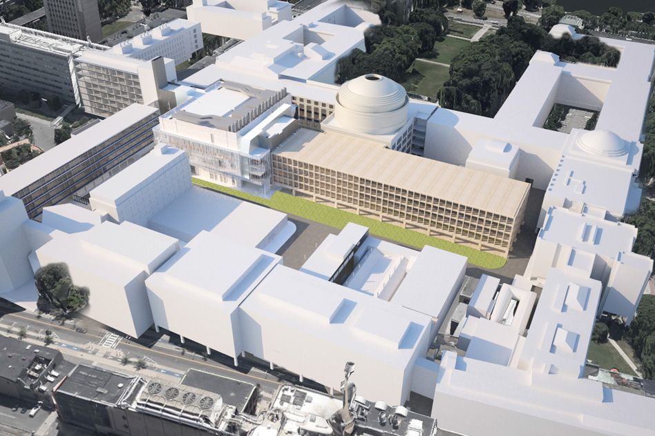
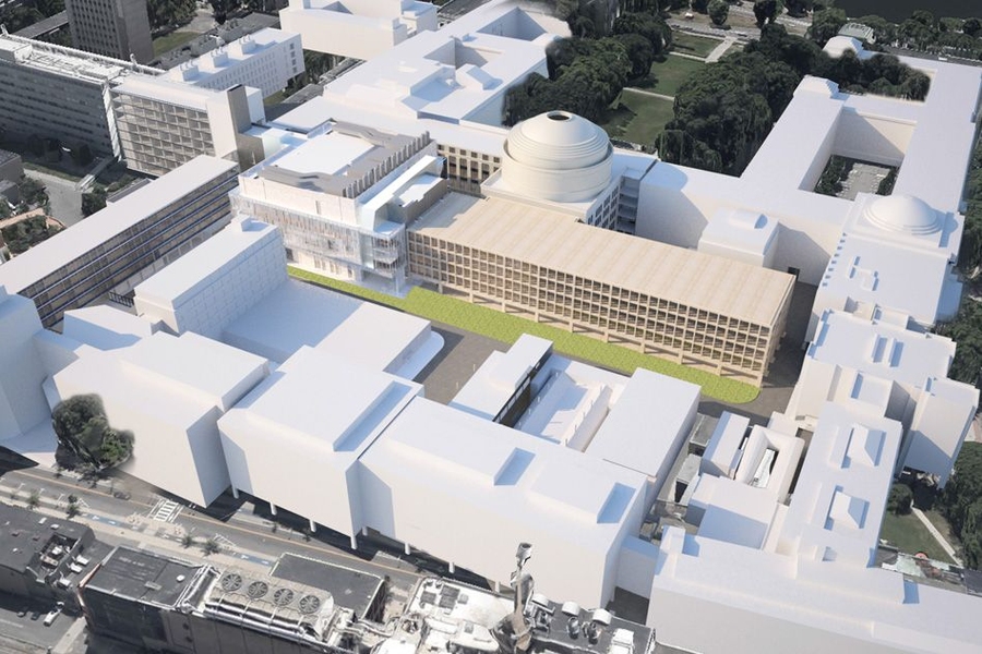
The four-level MIT.nano will replace the existing Building 12, and will retain its number, occupying a space alongside the iconic Great Dome. It will be interconnected with neighboring buildings, and accessible from MIT’s Infinite Corridor — meaning, Bulović says, that the new facility will be just a short walk from the numerous departments that will use its tools.
“This building needs to be centrally located, because nanoscale research is now central to so many disciplines,” says Bulović, who is the Fariborz Maseeh Professor in Emerging Technology at MIT.
Users of the new facility, he adds, are expected to come from more than 150 research groups at MIT. They will include, for example, scientists who are working on methods to “print” parts of human organs for transplantation; who are creating superhydrophobic surfaces to boost power-plant efficiency; who work with nanofluids to design new means of locomotion for machines, or new methods for purifying water; who aim to transform the manufacturing of pharmaceuticals; and who are using nanotechnology to reduce the carbon footprint of concrete, the world’s most ubiquitous building material.
PHOTOS: Watch a slide show illustrating areas of research that MIT.nano is expected to impact.
The research that will take place in MIT.nano could also help the world meet its growing energy needs, Bulović says. For example, cloud computing already consumes 1.3 percent of the world’s electricity; as this technology proliferates, its energy use is projected to grow a thousandfold over the coming decade. Hardware based on nanoscale switching elements — a new technology now being pursued by MIT researchers — could prove crucial in reducing the energy footprint of cloud computing.
“But we have many urgent challenges that existing technology cannot address,” Bulović says. “If we want to make sweeping change — more than incremental progress — in the most urgent technical areas, we need this building and the tools of nanoscience and nanotechnology housed within it.”
“The need for advanced facilities to support nanoscale research was identified in 2011 as the Institute’s highest academic priority as part of the MIT 2030 process to envision how our campus might evolve to meet future needs for research and education,” says Israel Ruiz, MIT’s executive vice president and treasurer. “It is wonderful to see we are boldly moving to accomplish our goal.”
Cleanroom facilities, by their nature, are among the most energy-intensive buildings to operate: Enormous air-handling machinery is needed to keep their air filtered to an extraordinarily high standard. Travis Wanat, the senior project manager at MIT who is overseeing the MIT.nano project, explains that while ventilation systems for ordinary offices or classrooms are designed to exchange the air two to six times per hour, cleanroom ventilation typically requires a full exchange 250 times an hour. The fans and filters necessary to handle this volume of air require an entire dedicated floor above each floor of cleanrooms in MIT.nano.
But MIT.nano will incorporate many energy-saving features: Richard Amster, director of campus engineering and construction, has partnered with Julie Newman, MIT’s director of sustainability. Together, they are working within MIT, as well as with the design and contracting teams, “to develop the most efficient building possible for cleanroom research and imaging,” Amster says.
Toward that end, MIT.nano will use heat-recovery systems on the building’s exhaust vents. The building will also be able to sense the local cleanroom environment and adjust the need for air exchange, dramatically reducing MIT.nano’s energy consumption. Dozens of other features aim to improve the building’s efficiency and sustainability.
Despite MIT.nano’s central location, the floor devoted to advanced imaging technology will have “more quiet space than anywhere on campus,” Bulović says: The facility is situated as far as possible from the noise of city streets and subway and train lines that flank MIT’s campus.
Indeed, protection from these sources of noise and mechanical vibration dictated the building’s location, from among five campus sites that were considered. According to national standards on ambient vibration, Bulović says, parts of MIT.nano will rate two levels better than the standard typically used for such high-quality imaging spaces.
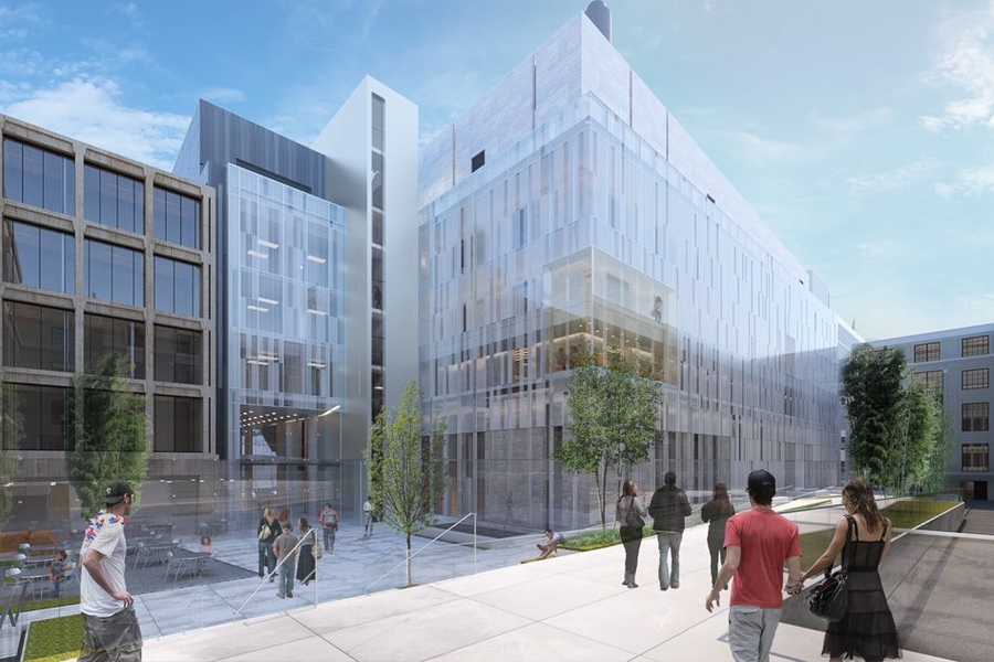
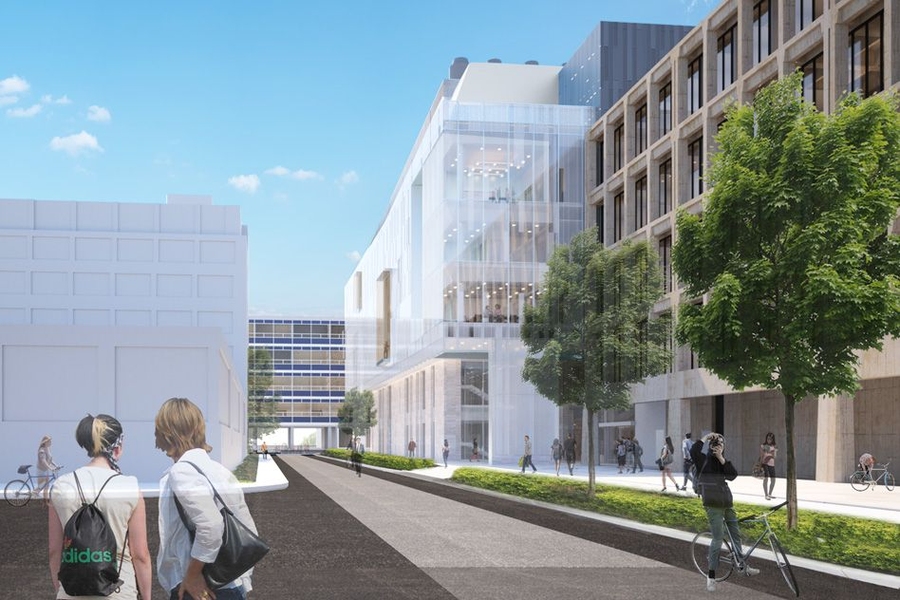
Another important goal of the building’s design — by Wilson Architects in Boston — is the creation of environments that foster interactions among users, including those from different disciplines. The building’s location at a major campus “crossroads,” its extensive use of glass walls that allow views into lab and cleanroom areas, and its soaring lobbies and other common areas are all intended to help foster such interactions.
“Nanoscale research is inherently interdisciplinary, and this building was designed to encourage collaboration,” Bulović says.
“MIT’s enduring leadership in technology and science is made possible by the interconnective nature of our community, and our total potential is greater than the sum of our parts,” adds Timothy Swager, the John D. MacArthur Professor of Chemistry. “At an intellectual level this is driven by our collective commitment to excellence and innovation, but the physical proximity of researchers at MIT is the heart and soul of this special atmosphere. MIT.nano will serve to enhance these interactions and provide an opportunity-rich venue where chemistry, biology, physics, and engineering all converge to create devices and understanding that will empower MIT researchers to reach new heights in innovation.”
The choice of MIT.nano’s central location is not without compromise, Bulović says: There is very limited access to the construction site — only three access roads, each with limited headroom — so planning for the activities of construction and delivery vehicles, and for the demolition of the current Building 12 and construction of MIT.nano, will present a host of logistical challenges. “It’s like building a ship in a bottle,” Bulović says.
But addressing those challenges will ultimately be well worth it, he says, pointing out that an estimated one-quarter of MIT’s graduate students and 20 percent of its researchers will make use of the facility. The new building “signifies the centrality of nanotechnology and nanomanufacturing for the needs of the 21st century. It will be a key innovation hub for the campus.”
All current occupants of Building 12 will be relocated by June, when underground facilities work, to enable building construction, will commence; at that point, fences will be erected around the constriction zone. The existing Building 12 will be demolished in spring 2015 and construction of MIT.nano is slated to begin in summer 2015.