


The next time you place your coffee order, imagine slapping onto your to-go cup a sticker that acts as an electronic decal, letting you know the precise temperature of your triple-venti no-foam latte. Someday, the high-tech stamping that produces such a sticker might also bring us food packaging that displays a digital countdown to warn of spoiling produce, or even a window pane that shows the day’s forecast, based on measurements of the weather conditions outside.
Engineers at MIT have invented a fast, precise printing process that may make such electronic surfaces an inexpensive reality. In a paper published today in Science Advances, the researchers report that they have fabricated a stamp made from forests of carbon nanotubes that is able to print electronic inks onto rigid and flexible surfaces.
A. John Hart, the Mitsui Career Development Associate Professor in Contemporary Technology and Mechanical Engineering at MIT, says the team’s stamping process should be able to print transistors small enough to control individual pixels in high-resolution displays and touchscreens. The new printing technique may also offer a relatively cheap, fast way to manufacture electronic surfaces for as-yet-unknown applications.
“There is a huge need for printing of electronic devices that are extremely inexpensive but provide simple computations and interactive functions,” Hart says. “Our new printing process is an enabling technology for high-performance, fully printed electronics, including transistors, optically functional surfaces, and ubiquitous sensors.”
Sanha Kim, a postdoc in MIT’s department of Mechanical Engineering, is the lead author, and Hart is the senior author. Their co-authors are Hossein Sojoudi, a postdoc in mechanical engineering and chemical engineering; Hangbo Zhao and Dhanushkodi Mariappan, graduate students in mechanical engineering; Gareth McKinley, the School of Engineering Professor of Teaching Innovation; and Karen Gleason, professor of chemical engineering and MIT’s associate provost.
A stamp from tiny pen quills
There have been other attempts in recent years to print electronic surfaces using inkjet printing and rubber stamping techniques, but with fuzzy results. Because such techniques are difficult to control at very small scales, they tend to produce “coffee ring” patterns where ink spills over the borders, or uneven prints that can lead to incomplete circuits.
“There are critical limitations to existing printing processes in the control they have over the feature size and thickness of the layer that’s printed,” Hart says. “For something like a transistor or thin film with particular electrical or optical properties, those characteristics are very important.”
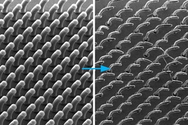
Hart and his team sought to print electronics much more precisely, by designing “nanoporous” stamps. (Imagine a stamp that’s more spongy than rubber and shrunk to the size of a pinky fingernail, with patterned features that are much smaller than the width of a human hair.) They reasoned that the stamp should be porous, to allow a solution of nanoparticles, or “ink,” to flow uniformly through the stamp and onto whatever surface is to be printed. Designed in this way, the stamp should achieve much higher resolution than conventional rubber stamp printing, referred to as flexography.
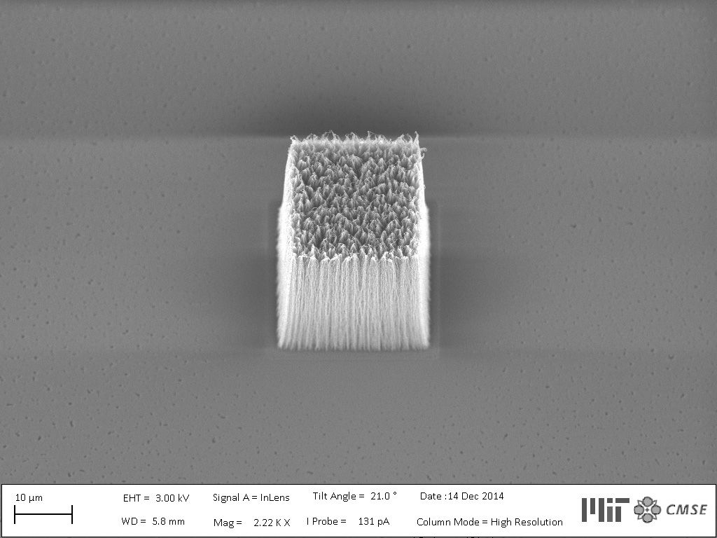
Kim and Hart hit upon the perfect material to create their highly detailed stamp: carbon nanotubes — strong, microscopic sheets of carbon atoms, arranged in cylinders. Hart’s group has specialized in growing forests of vertically aligned nanotubes in carefully controlled patterns that can be engineered into highly detailed stamps.
“It’s somewhat serendipitous that the solution to high-resolution printing of electronics leverages our background in making carbon nanotubes for many years,” Hart says. “The forests of carbon nanotubes can transfer ink onto a surface like massive numbers of tiny pen quills.”
Printing circuits, roll by roll
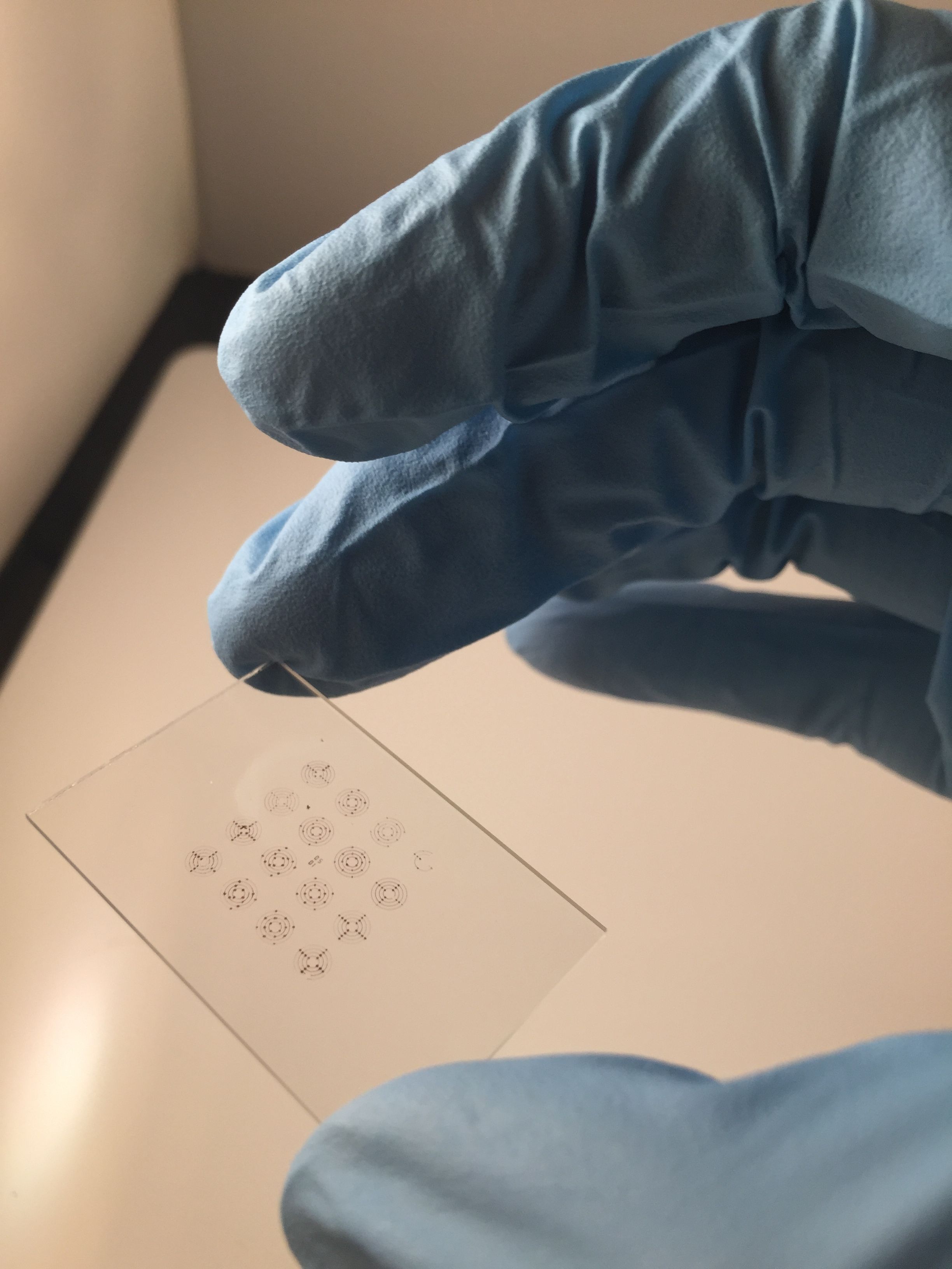
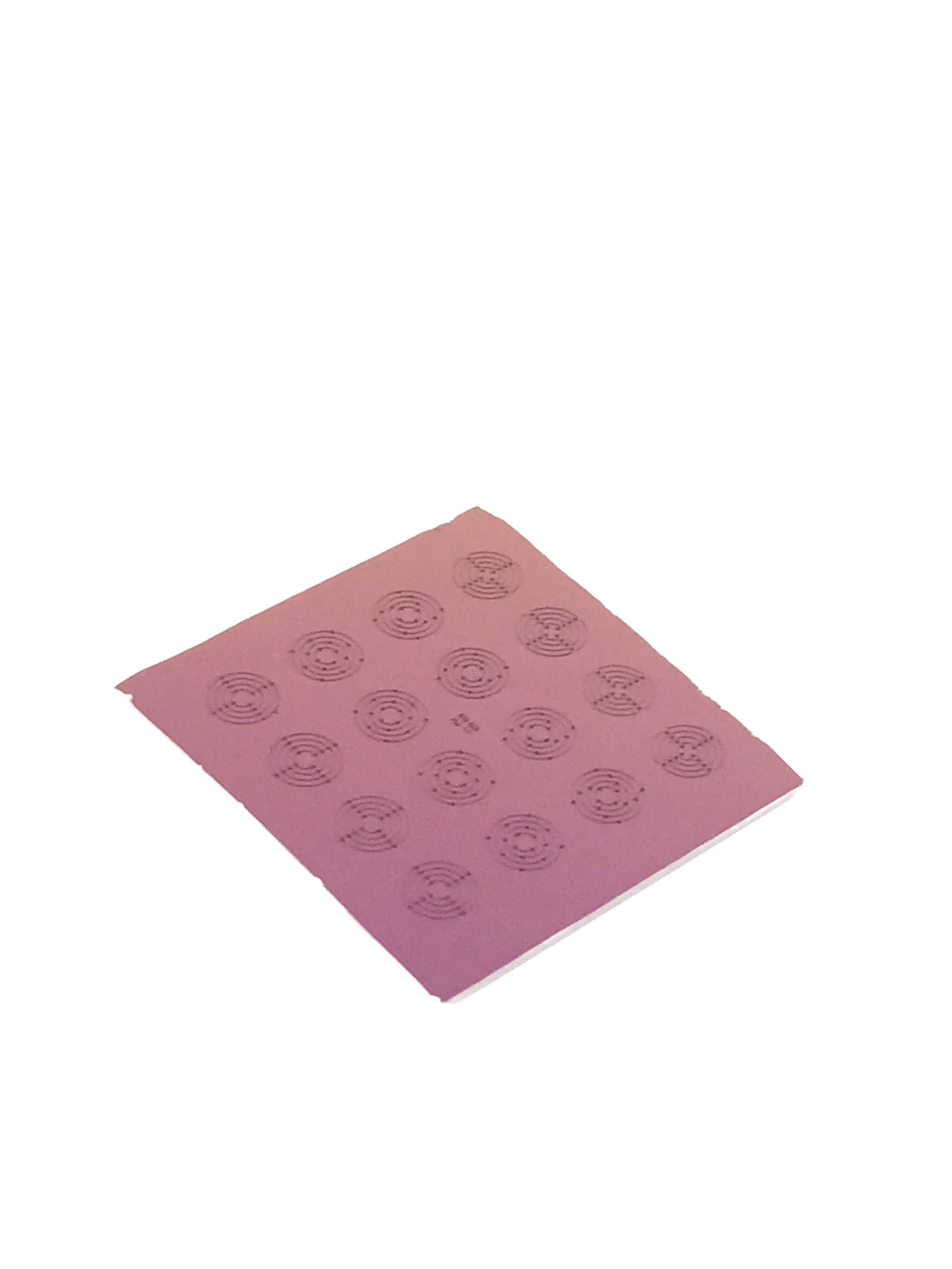
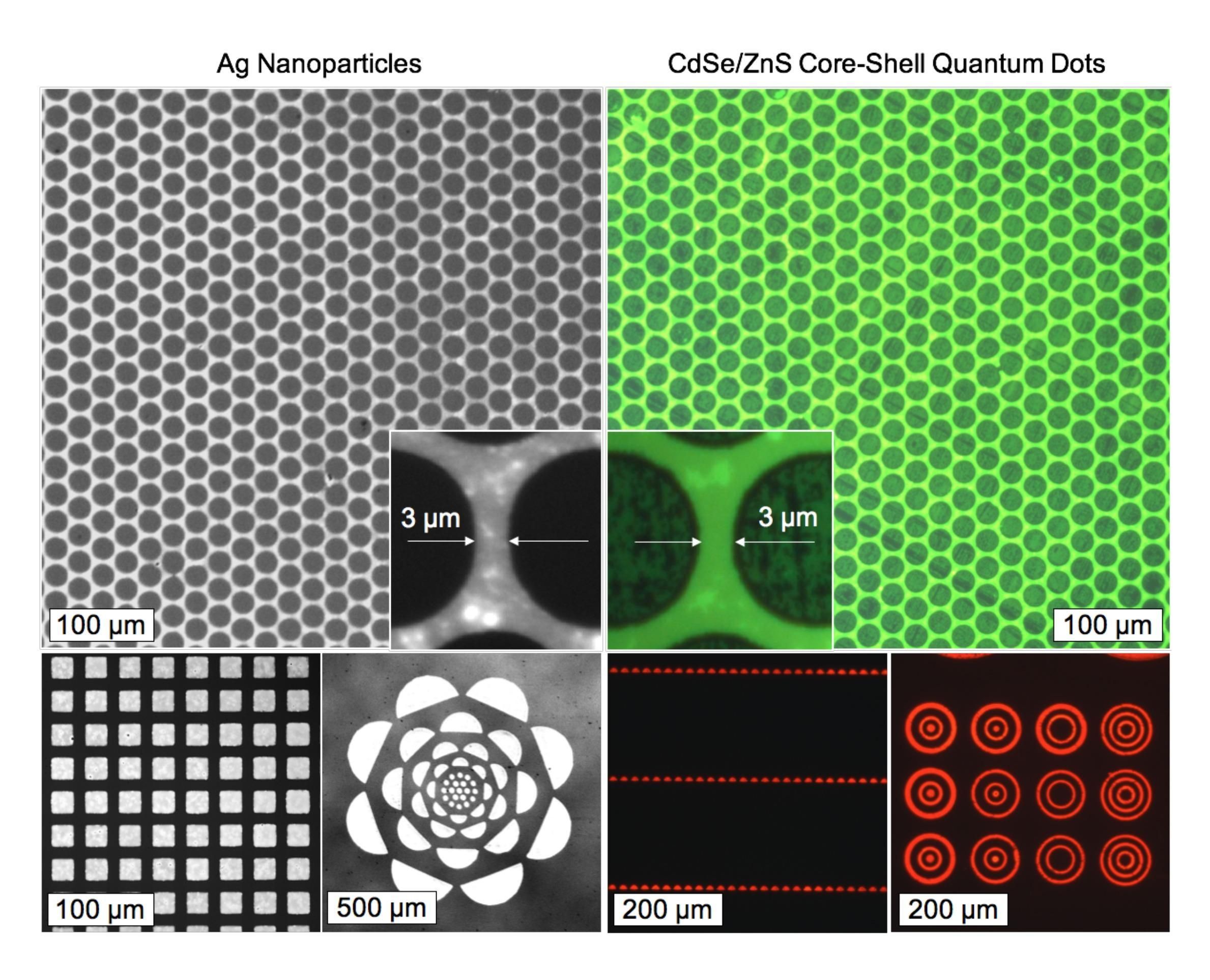
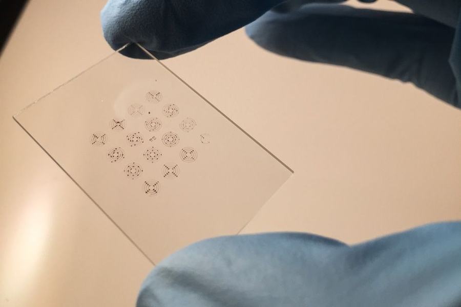
To make their stamps, the researchers used the group’s previously developed techniques to grow the carbon nanotubes on a surface of silicon in various patterns, including honeycomb-like hexagons and flower-shaped designs. They coated the nanotubes with a thin polymer layer (developed by Gleason’s group) to ensure the ink would penetrate throughout the nanotube forest and the nanotubes would not shrink after the ink was stamped. Then they infused the stamp with a small volume of electronic ink containing nanoparticles such as silver, zinc oxide, or semiconductor quantum dots.
The key to printing tiny, precise, high-resolution patterns is in the amount of pressure applied to stamp the ink. The team developed a model to predict the amount of force necessary to stamp an even layer of ink onto a substrate, given the roughness of both the stamp and the substrate, and the concentration of nanoparticles in the ink.
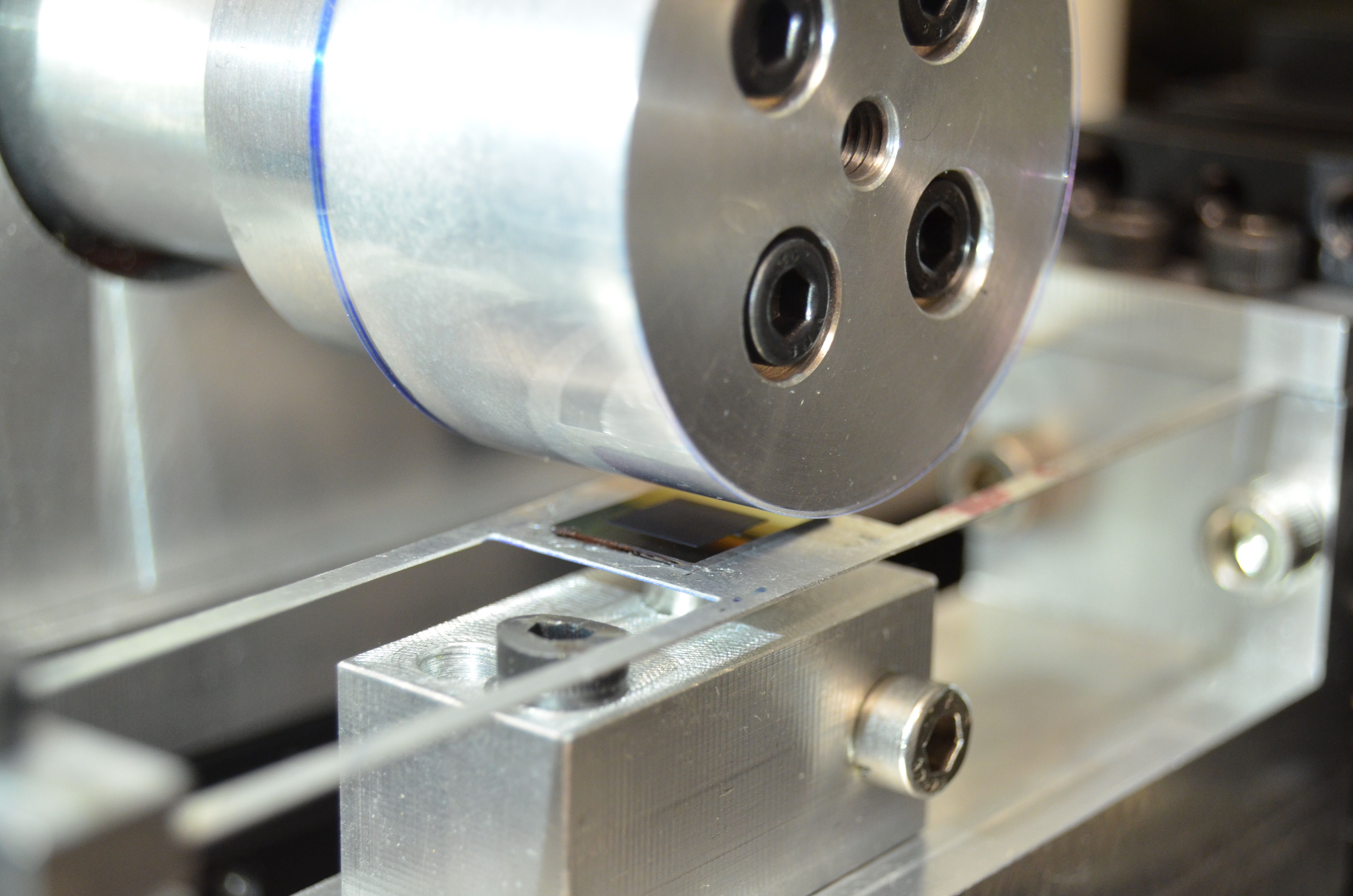
To scale up the process, Mariappan built a printing machine, including a motorized roller, and attached to it various flexible substrates. The researchers fixed each stamp onto a platform attached to a spring, which they used to control the force used to press the stamp against the substrate.
“This would be a continuous industrial process, where you would have a stamp, and a roller on which you’d have a substrate you want to print on, like a spool of plastic film or specialized paper for electronics,” Hart says. “We found, limited by the motor we used in the printing system, we could print at 200 millimeters per second, continuously, which is already competitive with the rates of industrial printing technologies. This, combined with a tenfold improvement in the printing resolution that we demonstrated, is encouraging.”
After stamping ink patterns of various designs, the team tested the printed patterns’ electrical conductivity. After annealing, or heating, the designs after stamping — a common step in activating electronic features — the printed patterns were indeed highly conductive, and could serve, for example, as high-performance transparent electrodes.
Going forward, Hart and his team plan to pursue the possibility of fully printed electronics.
“Another exciting next step is the integration of our printing technologies with 2-D materials, such as graphene, which together could enable new, ultrathin electronic and energy conversion devices,” Hart says.
This research was supported, in part, by the National Science Foundation and the MIT Energy Initiative.