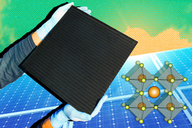
Perovskites are a family of materials that are currently the leading contender to potentially replace today’s silicon-based solar photovoltaics. They hold the promise of panels that are far thinner and lighter, that could be made with ultra-high throughput at room temperature instead of at hundreds of degrees, and that are cheaper and easier to transport and install. But bringing these materials from controlled laboratory experiments into a product that can be manufactured competitively has been a long struggle.
Manufacturing perovskite-based solar cells involves optimizing at least a dozen or so variables at once, even within one particular manufacturing approach among many possibilities. But a new system based on a novel approach to machine learning could speed up the development of optimized production methods and help make the next generation of solar power a reality.
The system, developed by researchers at MIT and Stanford University over the last few years, makes it possible to integrate data from prior experiments, and information based on personal observations by experienced workers, into the machine learning process. This makes the outcomes more accurate and has already led to the manufacturing of perovskite cells with an energy conversion efficiency of 18.5 percent, a competitive level for today’s market.
The research is reported today in the journal Joule, in a paper by MIT professor of mechanical engineering Tonio Buonassisi, Stanford professor of materials science and engineering Reinhold Dauskardt, recent MIT research assistant Zhe Liu, Stanford doctoral graduate Nicholas Rolston, and three others.
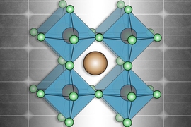
Perovskites are a group of layered crystalline compounds defined by the configuration of the atoms in their crystal lattice. There are thousands of such possible compounds and many different ways of making them. While most lab-scale development of perovskite materials uses a spin-coating technique, that’s not practical for larger-scale manufacturing, so companies and labs around the world have been searching for ways of translating these lab materials into a practical, manufacturable product.
“There's always a big challenge when you're trying to take a lab-scale process and then transfer it to something like a startup or a manufacturing line,” says Rolston, who is now an assistant professor at Arizona State University. The team looked at a process that they felt had the greatest potential, a method called rapid spray plasma processing, or RSPP.
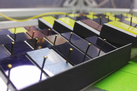
The manufacturing process would involve a moving roll-to-roll surface, or series of sheets, on which the precursor solutions for the perovskite compound would be sprayed or ink-jetted as the sheet rolled by. The material would then move on to a curing stage, providing a rapid and continuous output “with throughputs that are higher than for any other photovoltaic technology,” Rolston says.
“The real breakthrough with this platform is that it would allow us to scale in a way that no other material has allowed us to do,” he adds. “Even materials like silicon require a much longer timeframe because of the processing that's done. Whereas you can think of [this approach as more] like spray painting.”
Within that process, at least a dozen variables may affect the outcome, some of them more controllable than others. These include the composition of the starting materials, the temperature, the humidity, the speed of the processing path, the distance of the nozzle used to spray the material onto a substrate, and the methods of curing the material. Many of these factors can interact with each other, and if the process is in open air, then humidity, for example, may be uncontrolled. Evaluating all possible combinations of these variables through experimentation is impossible, so machine learning was needed to help guide the experimental process.
But while most machine-learning systems use raw data such as measurements of the electrical and other properties of test samples, they don’t typically incorporate human experience such as qualitative observations made by the experimenters of the visual and other properties of the test samples, or information from other experiments reported by other researchers. So, the team found a way to incorporate such outside information into the machine learning model, using a probability factor based on a mathematical technique called Bayesian Optimization.
Using the system, he says, “having a model that comes from experimental data, we can find out trends that we weren’t able to see before.” For example, they initially had trouble adjusting for uncontrolled variations in humidity in their ambient setting. But the model showed them “that we could overcome our humidity challenges by changing the temperature, for instance, and by changing some of the other knobs.”
The system now allows experimenters to much more rapidly guide their process in order to optimize it for a given set of conditions or required outcomes. In their experiments, the team focused on optimizing the power output, but the system could also be used to simultaneously incorporate other criteria, such as cost and durability — something members of the team are continuing to work on, Buonassisi says.
The researchers were encouraged by the Department of Energy, which sponsored the work, to commercialize the technology, and they’re currently focusing on tech transfer to existing perovskite manufacturers. “We are reaching out to companies now,” Buonassisi says, and the code they developed has been made freely available through an open-source server. “It’s now on GitHub, anyone can download it, anyone can run it,” he says. “We’re happy to help companies get started in using our code.”
Already, several companies are gearing up to produce perovskite-based solar panels, even though they are still working out the details of how to produce them, says Liu, who is now at the Northwestern Polytechnical University in Xi’an, China. He says companies there are not yet doing large-scale manufacturing, but instead starting with smaller, high-value applications such as building-integrated solar tiles where appearance is important. Three of these companies “are on track or are being pushed by investors to manufacture 1 meter by 2-meter rectangular modules [comparable to today’s most common solar panels], within two years,” he says.
‘The problem is, they don’t have a consensus on what manufacturing technology to use,” Liu says. The RSPP method, developed at Stanford, “still has a good chance” to be competitive, he says. And the machine learning system the team developed could prove to be important in guiding the optimization of whatever process ends up being used.
“The primary goal was to accelerate the process, so it required less time, less experiments, and less human hours to develop something that is usable right away, for free, for industry,” he says.
“Existing work on machine-learning-driven perovskite PV fabrication largely focuses on spin-coating, a lab-scale technique,” says Ted Sargent, University Professor at the University of Toronto, who was not associated with this work, which he says demonstrates “a workflow that is readily adapted to the deposition techniques that dominate the thin-film industry. Only a handful of groups have the simultaneous expertise in engineering and computation to drive such advances.” Sargent adds that this approach “could be an exciting advance for the manufacture of a broader family of materials” including LEDs, other PV technologies, and graphene, “in short, any industry that uses some form of vapor or vacuum deposition.”
The team also included Austin Flick and Thomas Colburn at Stanford and Zekun Ren at the Singapore-MIT Alliance for Science and Technology (SMART). In addition to the Department of Energy, the work was supported by a fellowship from the MIT Energy Initiative, the Graduate Research Fellowship Program from the National Science Foundation, and the SMART program.
