Costs of solar panels have plummeted over the last several years, leading to rates of solar installations far greater than most analysts had expected. But with most of the potential areas for cost savings already pushed to the extreme, further cost reductions are becoming more challenging to find.
Now, researchers at MIT and at the National Renewable Energy Laboratory (NREL) have outlined a pathway to slashing costs further, this time by slimming down the silicon cells themselves.
Thinner silicon cells have been explored before, especially around a dozen years ago when the cost of silicon peaked because of supply shortages. But this approach suffered from some difficulties: The thin silicon wafers were too brittle and fragile, leading to unacceptable levels of losses during the manufacturing process, and they had lower efficiency. The researchers say there are now ways to begin addressing these challenges through the use of better handling equipment and some recent developments in solar cell architecture.
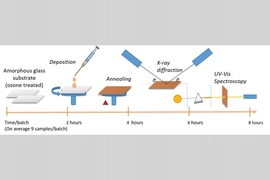
The new findings are detailed in a paper in the journal Energy and Environmental Science, co-authored by MIT postdoc Zhe Liu, professor of mechanical engineering Tonio Buonassisi, and five others at MIT and NREL.
The researchers describe their approach as “technoeconomic,” stressing that at this point economic considerations are as crucial as the technological ones in achieving further improvements in affordability of solar panels.
Currently, 90 percent of the world’s solar panels are made from crystalline silicon, and the industry continues to grow at a rate of about 30 percent per year, the researchers say. Today’s silicon photovoltaic cells, the heart of these solar panels, are made from wafers of silicon that are 160 micrometers thick, but with improved handling methods, the researchers propose this could be shaved down to 100 micrometers — and eventually as little as 40 micrometers or less, which would only require one-fourth as much silicon for a given size of panel.
That could not only reduce the cost of the individual panels, they say, but even more importantly it could allow for rapid expansion of solar panel manufacturing capacity. That’s because the expansion can be constrained by limits on how fast new plants can be built to produce the silicon crystal ingots that are then sliced like salami to make the wafers. These plants, which are generally separate from the solar cell manufacturing plants themselves, tend to be capital-intensive and time-consuming to build, which could lead to a bottleneck in the rate of expansion of solar panel production. Reducing wafer thickness could potentially alleviate that problem, the researchers say.
The study looked at the efficiency levels of four variations of solar cell architecture, including PERC (passivated emitter and rear contact) cells and other advanced high-efficiency technologies, comparing their outputs at different thickness levels. The team found there was in fact little decline in performance down to thicknesses as low as 40 micrometers, using today’s improved manufacturing processes.
“We see that there’s this area (of the graphs of efficiency versus thickness) where the efficiency is flat,” Liu says, “and so that’s the region where you could potentially save some money.” Because of these advances in cell architecture, he says, “we really started to see that it was time to revisit the cost benefits.”
Changing over the huge panel-manufacturing plants to adapt to the thinner wafers will be a time-consuming and expensive process, but the analysis shows the benefits can far outweigh the costs, Liu says. It will take time to develop the necessary equipment and procedures to allow for the thinner material, but with existing technology, he says, “it should be relatively simple to go down to 100 micrometers,” which would already provide some significant savings. Further improvements in technology such as better detection of microcracks before they grow could help reduce thicknesses further.
In the future, the thickness could potentially be reduced to as little as 15 micrometers, he says. New technologies that grow thin wafers of silicon crystal directly rather than slicing them from a larger cylinder could help enable such further thinning, he says.
Development of thin silicon has received little attention in recent years because the price of silicon has declined from its earlier peak. But, because of cost reductions that have already taken place in solar cell efficiency and other parts of the solar panel manufacturing process and supply chain, the cost of the silicon is once again a factor that can make a difference, he says.
“Efficiency can only go up by a few percent. So if you want to get further improvements, thickness is the way to go,” Buonassisi says. But the conversion will require large capital investments for full-scale deployment.
The purpose of this study, he says, is to provide a roadmap for those who may be planning expansion in solar manufacturing technologies. By making the path “concrete and tangible,” he says, it may help companies incorporate this in their planning. “There is a path,” he says. “It’s not easy, but there is a path. And for the first movers, the advantage is significant.”
What may be required, he says, is for the different key players in the industry to get together and lay out a specific set of steps forward and agreed-upon standards, as the integrated circuit industry did early on to enable the explosive growth of that industry. “That would be truly transformative,” he says.
Andre Augusto, an associate research scientist at Arizona State University who was not connected with this research, says “refining silicon and wafer manufacturing is the most capital-expense (capex) demanding part of the process of manufacturing solar panels. So in a scenario of fast expansion, the wafer supply can become an issue. Going thin solves this problem in part as you can manufacture more wafers per machine without increasing significantly the capex.” He adds that “thinner wafers may deliver performance advantages in certain climates,” performing better in warmer conditions.
Renewable energy analyst Gregory Wilson of Gregory Wilson Consulting, who was not associated with this work, says “The impact of reducing the amount of silicon used in mainstream cells would be very significant, as the paper points out. The most obvious gain is in the total amount of capital required to scale the PV industry to the multi-terawatt scale required by the climate change problem. Another benefit is in the amount of energy required to produce silicon PV panels. This is because the polysilicon production and ingot growth processes that are required for the production of high efficiency cells are very energy intensive.”
Wilson adds “Major PV cell and module manufacturers need to hear from credible groups like Prof. Buonassisi’s at MIT, since they will make this shift when they can clearly see the economic benefits.”
The team also included Sarah Sofia, Hannu Lane, Sarah Wieghold and Marius Peters at MIT and Michael Woodhouse at NREL. The work was partly supported by the U.S. Department of Energy, the Singapore-MIT Alliance for Research and Technology (SMART), and by a Total Energy Fellowship through the MIT Energy Initiative.