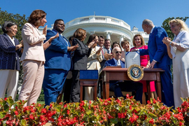


To celebrate the passage of the CHIPS and Science Act of 2022 — which authorizes major funding increases for scientific research and provides about $52 billion for U.S. semiconductor research, development, and manufacturing — Sen. Elizabeth Warren paid a visit to MIT’s state-of-the-art facility for nanoscale science and engineering on Wednesday.
She arrived at MIT.nano, a shared 214,000-square-foot nanoscale research center located in the heart of campus, one day after President Joe Biden signed the bipartisan measure into law. The act aims to help the U.S. reassert its leadership in microelectronics research, development, and manufacturing, while also expanding the semiconductor workforce. It also authorizes significantly expanded funding for the National Science Foundation, where a new Technology, Innovation, Partnerships Directorate will be established.
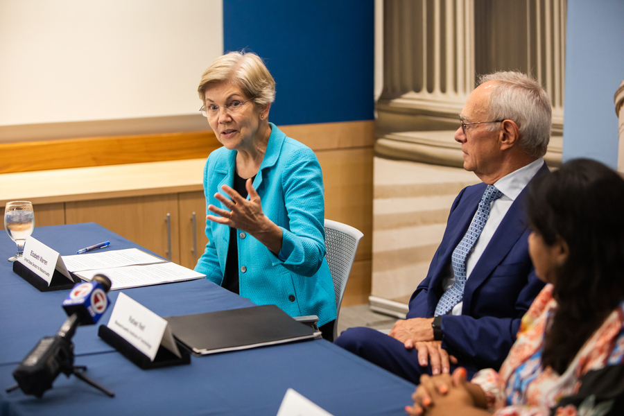
“I believe our job in Washington is to build for the future,” Warren said, addressing a roundtable of university leaders after she toured the MIT.nano facility. “I am delighted about $52 billion that is going into chips, that is going into domestic manufacturing, that is going into strengthening our supply chains. But keep in mind … we’ve [also got billions] going directly into increasing the budget of the National Science Foundation. That has the potential to be transformative.”
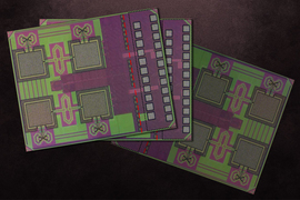
Semiconductors are critical components of consumer goods like cars and appliances, but also medical technology, industrial equipment, and military systems. The U.S. produced nearly 40 percent of the world’s semiconductors in 1990, but that had fallen to around 12 percent by 2020, according to the Semiconductor Industry Association.
A shortage of semiconductor chips, brought on largely by the Covid-19 pandemic, led to production bottlenecks that have helped fuel record U.S. inflation. Reasserting U.S. leadership in microelectronics, which is important for the nation’s economic growth and defense, was the topic of an MIT white paper released earlier this year.
“At MIT, we are proud to support this national effort in research and education. … As nations around the world understand very well, future competitiveness, prosperity, and national security all rely on technological leadership,” said MIT President L. Rafael Reif, speaking at the start of the roundtable discussion. “To sustain strength in the long-term, the U.S. needs to invent and manufacture the next new technologies, and this bill supplies a springboard to those as yet-undreamed-of innovations.”
Reif also underscored the law’s emphasis on “use-inspired basic research” — fundamental research targeted at solving practical problems, like the research that led to the invention of the semiconductor in the 1940s. Reif was a strong advocate for making support of such research across a range of fields a prominent feature of the CHIPS and Science Act. He and Warren met privately at the start of her visit to discuss next steps for implementing the NSF portion of the legislation, and other federal issues.
The group then proceeded on a tour of the MIT.nano facility, led by Vladimir Bulović, the faculty director of MIT.nano and Fariborz Maseeh Chair in Emerging Technology. The tour was designed to highlight aspects of microelectronics research and education that could be augmented through the new law.
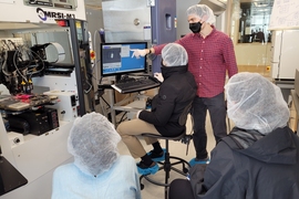
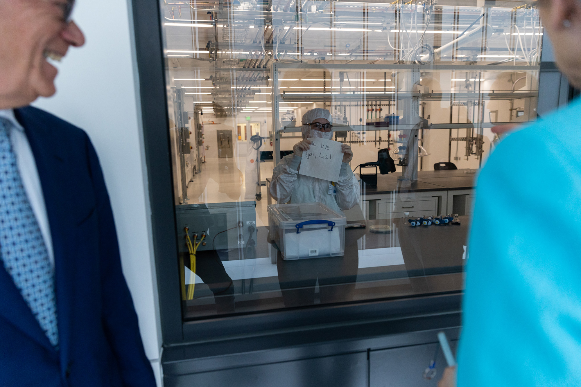
The first stop was a view into the MIT.nano cleanroom and a conversation with Jesús del Alamo, the Donner Professor of Electrical Engineering and Computer Science, and Mark Gouker, the assistant division head of advanced technology at MIT Lincoln Laboratory.
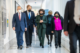
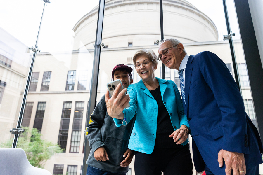
Warren, also joined by her husband, Bruce H. Mann, and her grandson, peered through a window into the cleanroom, a controlled environment where airborne particles are filtered out, watching as researchers in protective clothing utilized sophisticated tools to manipulate nanoscale materials. Del Alamo, Bulović, and Gouker explained that the MIT research scientists, postdoctoral and graduate fellows, and undergraduate students have opportunities to use this cutting-edge equipment for innovation and education. They also discussed how researchers across the U.S. and around the world can take advantage of the state-of-the-art, open-access facilities to advance their work.
On the lower level of MIT.nano, Warren and the others watched atoms moving on the screen of a Hitachi HF5000 field emission transmission electron microscope. Frances Ross, the Ellen Swallow Richards Professor in Materials Science and Engineering, explained how the state-of-the-art microscope enables researchers to observe atoms and their behavior, which is key to understanding the properties of novel materials. These materials could be used to develop more powerful and energy-efficient electronic devices in the future.
As the tour continued, Warren met with representatives from the Massachusetts Technology Collaborative and Analog Devices, who emphasized how important infrastructure and collaboration are for enabling innovation. She also met with founders of two startups born at MIT, Atlantic Quantum and Active Surfaces, both of which have extensively used MIT.nano facilities.
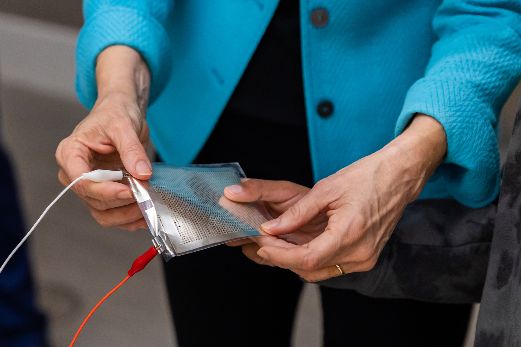
As he talked about his company, Richard Swartwout PhD ’21, CEO and founder of Active Surfaces, handed Warren what looked like a sheet of aluminum foil. She laughed out loud when the sheet, which is actually a paper-thin loudspeaker, began playing a song by country music singer Patsy Cline. (Cline’s “Showcase” was the first album Warren ever bought.)
Warren also talked about STEM workforce development with Drew Weninger, SM ’21, a graduate research fellow in the Electronic Materials Research Group and a member of MIT LEAP (Lab for Education and Application Prototypes), which seeks, in part, to rapidly train photonics manufacturing technicians.
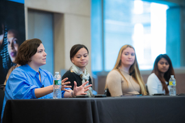
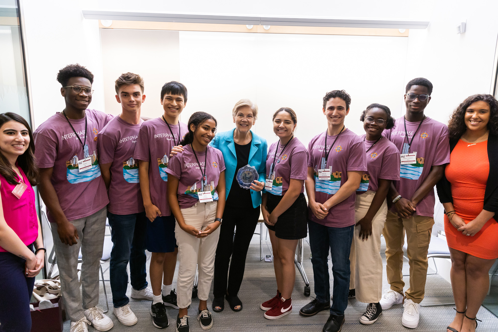
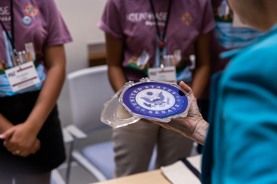
She also met with a group of incoming first-year students who are participating in the Interphase EDGE program, a summer program that includes experiences working in the MIT.nano cleanroom. The students presented her with a silicon wafer imprinted with the seal of the U.S. Senate, which they had made in the cleanroom using the same techniques that produce semiconductor chips.
At the conclusion of the tour, Warren participated in a roundtable discussion to which she had invited leaders from local universities on the significance of the CHIPS and Science Act. The roundtable included Reif, Jean Morrison, university provost and chief academic officer at Boston University; Steven F. Karel, vice provost for research at Brandeis University; John Shaw, vice provost for research at Harvard University; David Luzzi, senior vice provost for research at Northeastern University; Julie Chen, chancellor of the University of Massachusetts at Lowell; Lynn Perry Wooten, president of Simmons University; Carl A. Rust, executive director of industry engagement and business development at the University of Massachusetts System; Winston Oluwole Soboyejo, interim president at Worcester Polytechnic Institute; Peter Hill, director of government relations at the Woods Hole Oceanographic Institution; and Sumbul Siddiqui, mayor of the City of Cambridge.
The university leaders emphasized important elements of the bill beyond R&D funding, including a provision that tightens the rules addressing sexual harassment in science, and the funding it could provide to encourage more women and underrepresented minorities to pursue STEM fields. Those elements will be key to building a stronger technical workforce, they said.
Warren agreed, saying, “We can’t afford to leave segments of the population behind.”
The bill will also help universities support graduate students and encourage potential students, including those in high school or middle school, to consider careers in research and manufacturing.
Warren said she especially enjoyed interacting with incoming first-year students, and that for her, the visit emphasized the important role universities will play in boosting U.S. leadership in microelectronics.