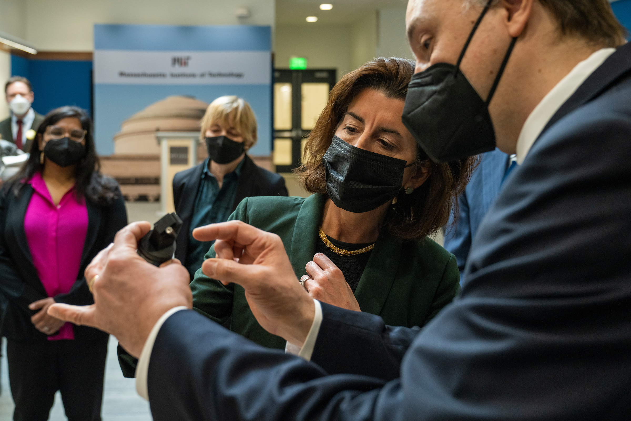

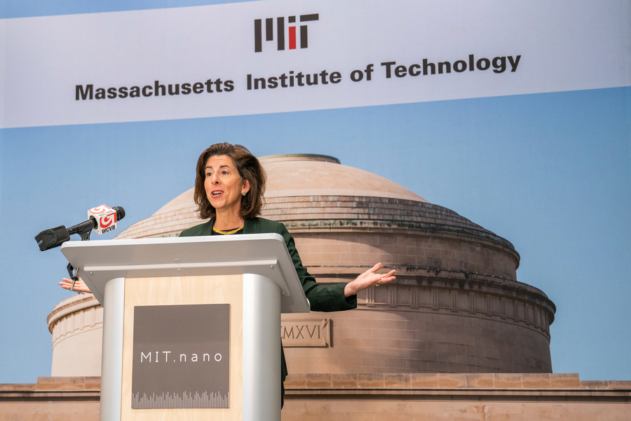
The global semiconductor shortage, a major driver of ballooning U.S. inflation, is as much a national security issue as an economic issue, U.S. Secretary of Commerce Gina Raimondo said during a recent visit to MIT.
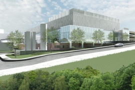
Speaking at MIT.nano, a shared 214,000-square-foot research center for nanoscale science and engineering located in the heart of campus, Raimondo said that not long ago, the U.S. produced about 40 percent of the world’s semiconductors. Today, the nation makes only about 12 percent.
By producing more semiconductors domestically, the U.S. could drive down the costs of the countless consumer goods that contain chips, and limit its reliance on imported semiconductors, especially highly advanced chips for military equipment.
“No one can outcompete the United States of America if we invest in our people, like the students and scientists who are here [at MIT], and get back to the business of investing in basic science. America has lost its way in the past few decades as it relates to manufacturing, and we need to get back there. And that begins with R&D,” she said.
Raimondo traveled to campus to tour MIT.nano the day after President Biden’s State of the Union Address, in which he emphasized the critical role semiconductor research and manufacturing plays in creating good jobs and leveling the technological playing field between the U.S. and China. During his address, Biden urged Congress to pass the innovation act, legislation that would, among other things, provide $52 billion to the Department of Commerce to invest in domestic semiconductor manufacturing. The House passed their version of the legislation in February, while the Senate had passed their version in June. The two chambers must now work out a compromise.
Raimondo stressed how the Commerce Department’s investment would leverage both industry and universities to ensure the U.S. leads again in domestic production of semiconductors. A group of MIT researchers recently published a white paper that lays out a strategy for how universities can support that effort.
In opening remarks, Sumbul Siddiqui, mayor of the City of Cambridge, described the role of Cambridge and MIT in supporting critical domestic research and development.
“The U.S. has long been a beacon of excellence in science and technology in the world, but we need to reinvest in scientific research and continue to grow innovation hubs like Cambridge, and to ensure the U.S. stays competitive globally. And MIT plays a key role in that,” Siddiqui said before introducing MIT President L. Rafael Reif.
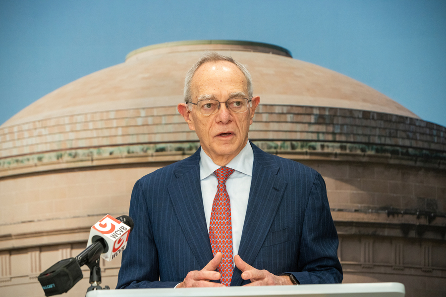
As he welcomed Raimondo to campus, Reif also emphasized the importance of the innovation act.
“That legislation will be a powerful accelerant for the whole spectrum of semiconductor research and development, from advancing the work of university labs to helping the U.S. rebuild its leadership in semiconductor manufacturing. MIT is proud to play a part in this larger effort, by conducting semiconductor research, educating the kind of inspiring students you met today, and producing innovations and helping them get to market,” Reif said.
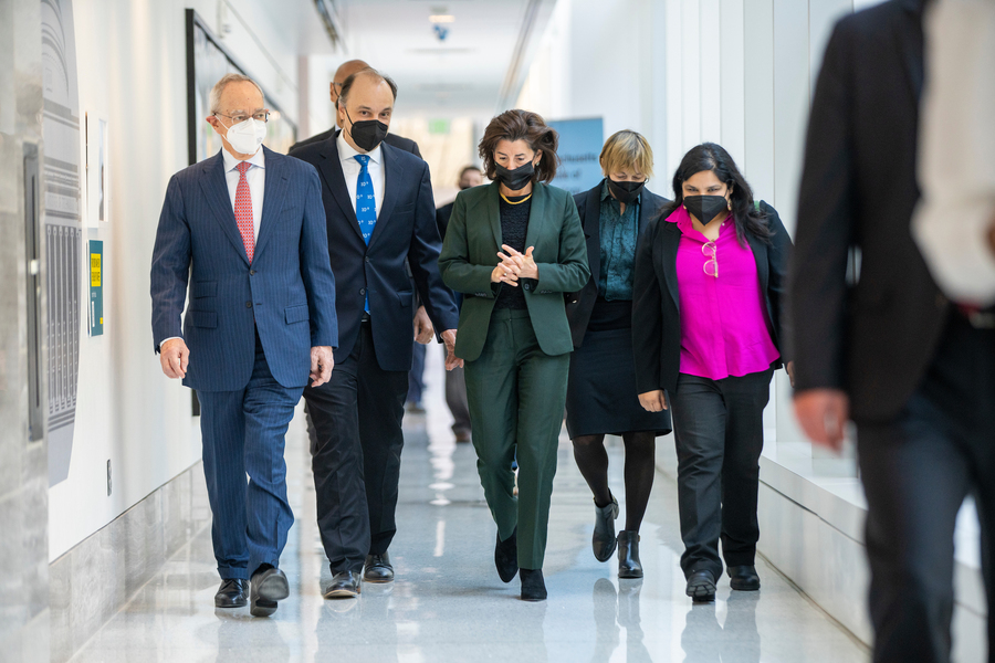
Raimondo was able to see examples of all three of those aspects — research, education, and commercialization — during a tour of the MIT.nano facility. The tour was led by Reif; Maria Zuber, MIT’s vice president for research; Vladimir Bulović, faculty director of MIT.nano and Fariborz Maseeh Chair in Emerging Technology; Jesús del Alamo, Donner Professor of Electrical Engineering and Computer Science; and Robert Atkins, division head of advanced technology at MIT Lincoln Laboratory.
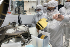
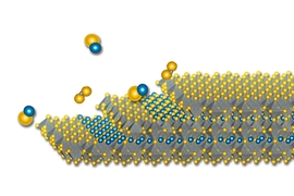
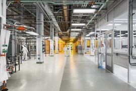
The first stop was a view into the MIT.nano cleanroom, the pristine laboratory environment for fabricating semiconductors and other nano- and microtechnologies. As a team of students worked with sophisticated tools on the other side of the window to deposit nanoscale patterns on a silicon wafer, Reif and Bulović discussed with Raimondo the critical need to support innovations in hardware at a time when developments in software often take center stage.
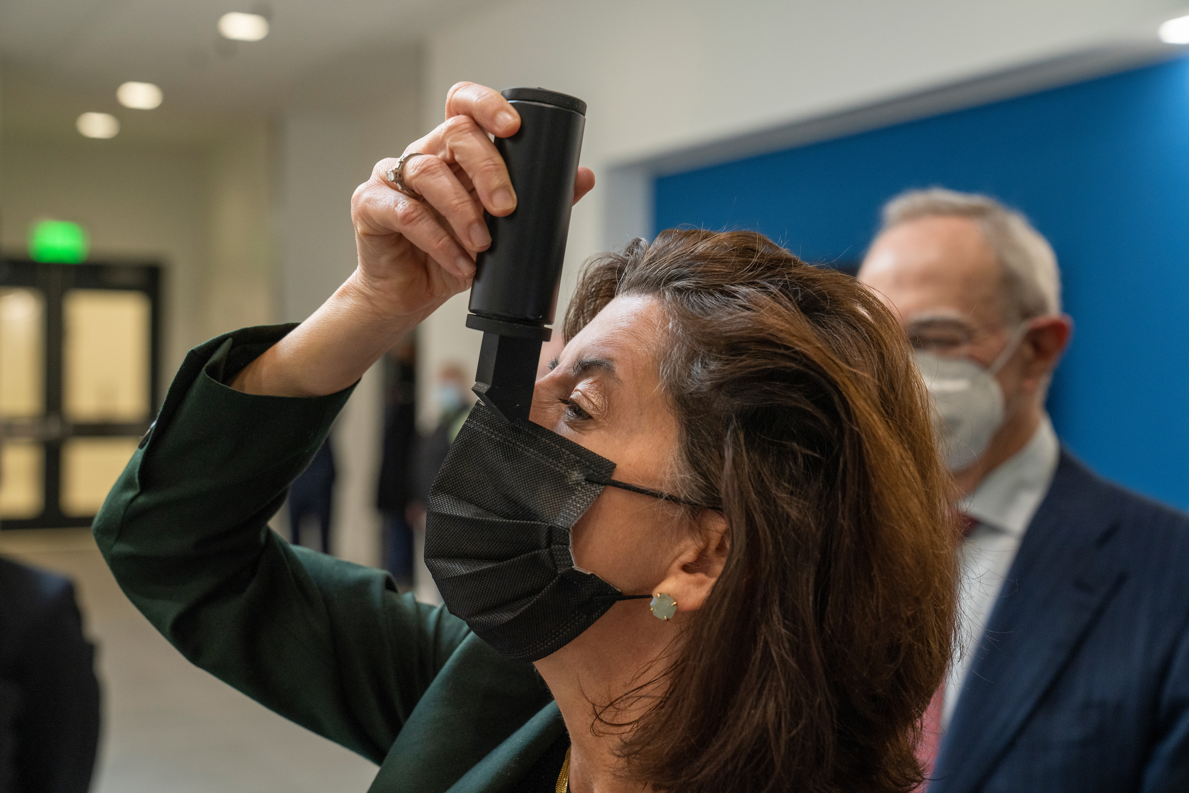
Raimondo and the others on the tour moved on to the lower level of MIT.nano, which houses a suite of powerful microscopes and other imaging instrumentation for seeing and measuring at the nanoscale, such as the Hitachi HF5000 field emission transmission electron microscope, which is newly acquired by the facility.
Upon entering the room where the 12-foot-tall instrument sits, Bulović announced that “we are at the dawn of the nano age” thanks to instruments like the Hitachi that enable scientists to look at individual atoms.
Frances Ross, the Ellen Swallow Richards Professor in Materials Science and Engineering, explained to Raimondo that being able to see individual atoms could help researchers learn how to control the properties of ultrathin materials and use them in new electronic devices. This technology could also enable scientists to redesign catalyst particles so they could speed chemical reactions without the need for costly rare-earth materials or find more environmentally friendly alternatives to batteries.
Impressed by the scientific possibilities this high-tech microscope affords, Raimondo said those types of applications are “critical to our national security.”
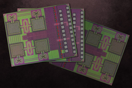
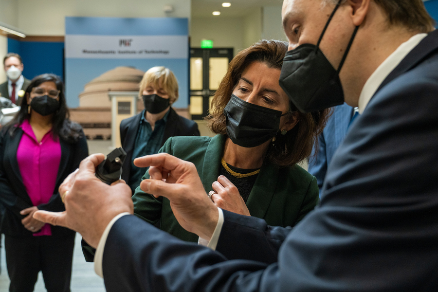
The tour then moved on to a showcase of technology prototypes where Raimondo saw some cutting-edge devices up-close. Atkins presented an 8-inch silicon wafer for superconducting electronics, built at MIT Lincoln Laboratory, that consumes about 100 times less power than traditional computer hardware.
To highlight MIT.nano’s role in facilitating entrepreneurial activity, Brendan Smith, PhD ’18, CEO and co-founder of SiTration, showcased his startup’s membrane filtration devices. The technology, which Smith worked on while he was a PhD student at MIT, uses precisely sized nanopores in silicon wafers to isolate liquids and gases for the chemical separation industry, using 10 times less energy than current processes. Smith called the opportunity to use MIT.nano facilities a “game changer” for an early-stage company.
Smith, who participated in the START.nano accelerator, was able to use MIT.nano as both a student and an alumnus. About 10 to 15 percent of MIT.nano users are outside the Institute — in addition to faculty members, researchers, and students, qualified users from industry, academia, and government can work on projects at MIT.nano with the support of the facility’s technical staff.
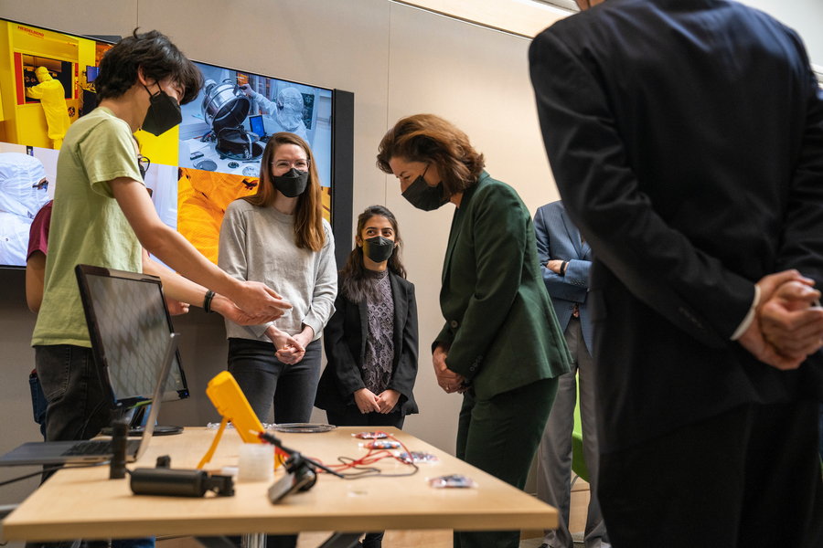
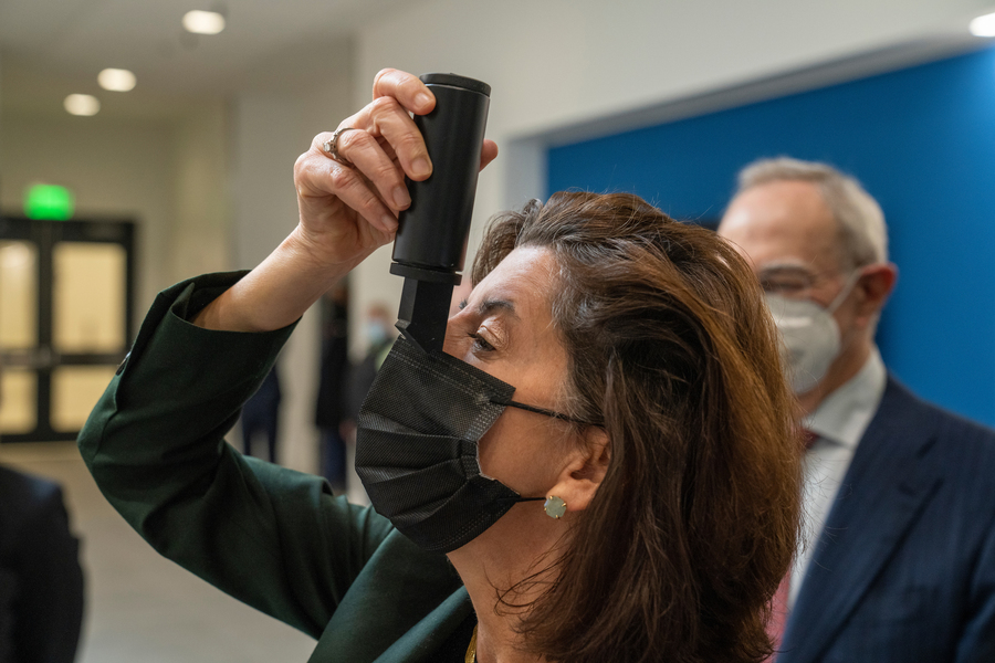
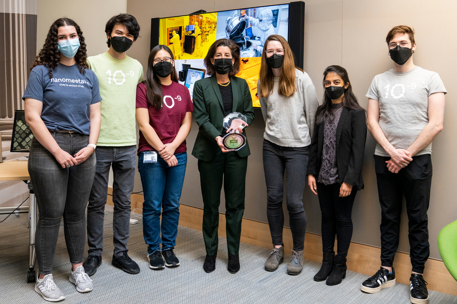
Raimondo also met several MIT undergraduates who had the opportunity to work in MIT.nano. The students demonstrated a spectrometer and explained how it could be used to detect Covid-19. First-year students Kevin Kurashima and Audrey Lee showed Raimondo solar panels they fabricated in the new course 6.A06 (First.nano! – Fabricate Your Own Solar Cell in MIT.nano Cleanroom). In this course, first-year students spent three hours in MIT.nano facilities each week, experimenting with nanotechnology tool sets and building silicon solar cells.
Course instructor del Alamo said one goal of the course is to give first-year students a glimpse inside MIT.nano early so they can start working on research projects sooner in their academic careers. It is already paying off — Kurashima has since joined del Alamo’s research group.
Educating students about nanotechnology and semiconductors before they reach high school will be critical for building up the workforce needed for the U.S. to massively boost domestic semiconductor manufacturing, Bulović told Raimondo.
“These individuals are the workforce of tomorrow, and we need many more of them,” Bulović said. In answer to a question from Raimondo, Bulović remarked that students don’t need a PhD to do this work, rather “they just need to know that it is possible.”
Ultimately, Raimondo said that meeting the students, and feeling their enthusiasm about microelectronics research and development, impressed her the most during her visit.
“Sometimes, we fall into the tendency to get a little down because of what we see going on in the world. Coming to a place like this is really invigorating. To see what is happening, to see the United States of America leading in the areas that we need to lead, to see these facilities and know that they are open to the community, essentially, gives me tremendous hope and optimism that we are going to solve our problems,” she said.