MIT engineers report creating the first high-quality thin films of a new family of semiconductor materials. The feat, which lead researcher Rafael Jaramillo refers to as his “white whale” because of his obsession in pursuing it over the years, has the potential to impact multiple fields of technology if history repeats itself. The ability to create high-quality films of other families of semiconductors led to computers, solar cells, night-vision cameras, and more.
When introducing a new material, “the most important scientific breakthroughs are enabled only when we have access to the highest-quality materials available,” says Jaramillo, the Thomas Lord Associate Professor of Materials Science and Engineering at MIT. “Studying materials of low quality often results in false negatives with respect to their scientific interest and technological potential.”
The new family of semiconductors, known as chalcogenide perovskites, could have applications in solar cells and lighting, Jaramillo says. He notes, however, that “the history of semiconductor research shows that new families of semiconductors are generally enabling in ways that are not predictable.”
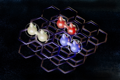
Jaramillo is excited about the new materials’ potential because they are ultrastable and made of inexpensive, nontoxic elements. The thin films his team created are composed of barium, zirconium, and sulfur in a specific crystal structure, “the prototypical chalcogenide perovskite,” Jaramillo says. “You can make variations by changing the composition. So it is indeed a family of materials, not just a one-off.”
The work has been published in the Nov. 3 issue of Advanced Functional Materials. Jaramillo’s coauthors are Ida Sadeghi, a postdoc in the Department of Materials Science and Engineering (DMSE) and first author of the paper; Kevin Ye, Michael Xu, and Yifei Li, all DMSE graduate students; and James M. LeBeau, the John Chipman Associate Professor of Materials Science and Engineering at MIT.
A little history
Chalcogenide perovskites were made as early as the 1950s by French chemists. Similar work was repeated in the 80s and early 90s, but “the idea that these materials would be useful semiconductors didn’t come along until the early 2010s,” Jaramillo says. That’s when Jaramillo and a few others — including Jayakanth Ravichandran and Joseph Bennett, all postdocs at the time — independently identified their potential.
Today, Ravichandran and Bennett are professors at the University of Southern California and the University of Maryland Baltimore County, respectively; Jaramillo counts both as friends. Ravichandran, who Jaramillo met when the two were postdocs at Harvard University, has also pursued the goal of creating high-quality chalcogenide perovskite films, albeit using a different approach. Ravichandran has also continued with success in this field.
How they did it
Jaramillo and colleagues used a technique called molecular beam epitaxy (MBE) to grow their high-quality films. The technique allows atomic-level control over crystal growth, but “it’s extremely hard to do and there’s no guarantee of success [with a new material],” Jaramillo says. Nevertheless, “the history of semiconductor technology shows the value of developing MBE. That’s why it’s worthwhile to try.”
As its name implies, MBE essentially points beams of molecules at a specific arrangement of atoms on a surface (“taxy,” as in epitaxy, means arrangement, or orientation). That arrangement of atoms provides a template for the beamed molecules to grow on. “That’s why epitaxial growth gives you the highest-quality films. The materials know how to grow,” Jaramillo says.
The difficult work was further compounded by another factor: “the chemicals needed to make chalcogenides are nasty. They stink, and they can gum up equipment,” Jaramillo says. MBE takes place in a vacuum chamber, and Jaramillo recalls the reluctance of people to allow his group access to their chambers.
Says Hideo Hosono, a professor at the Tokyo Institute of Technology who was not involved in the work, “the thin films [created by Jaramillo et al.] show a mirror-smooth image as a result of an atomically flat surface, and excellent quality. We may anticipate the realization of device fabrication such as solar cells and green LEDs as the next publications.”
What’s next?
“It’s almost a question of what isn’t next,” Jaramillo says. “Now that we can make these high-quality materials, there’s almost no measurement we could do that wouldn’t be interesting to a wide community of people.” For now, his group is focusing on two areas: exploring fundamental questions to gain a better understanding of the materials, and integrating them into solar cells. In one of his postdoctoral appointments before joining the MIT faculty, Jaramillo worked on solar cells, so “I’ll be able to leverage a lot of what I did then.”
Chalcogenide perovskites are not the sole focus of Jaramillo’s lab at MIT. “But this is definitely the project we’re proudest of because it’s taken the most effort and the most delayed gratification.”
This work was supported by the National Science Foundation, the Office of Naval Research, the Skolkovo Institute of Science and Technology as part of the MIT-Skoltech Next Generation Program, and the Air Force Office of Scientific Research.
Facilities managed by the MIT Materials Research Laboratory and by MIT.nano were used for part of the work.