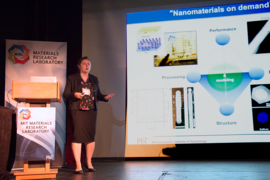
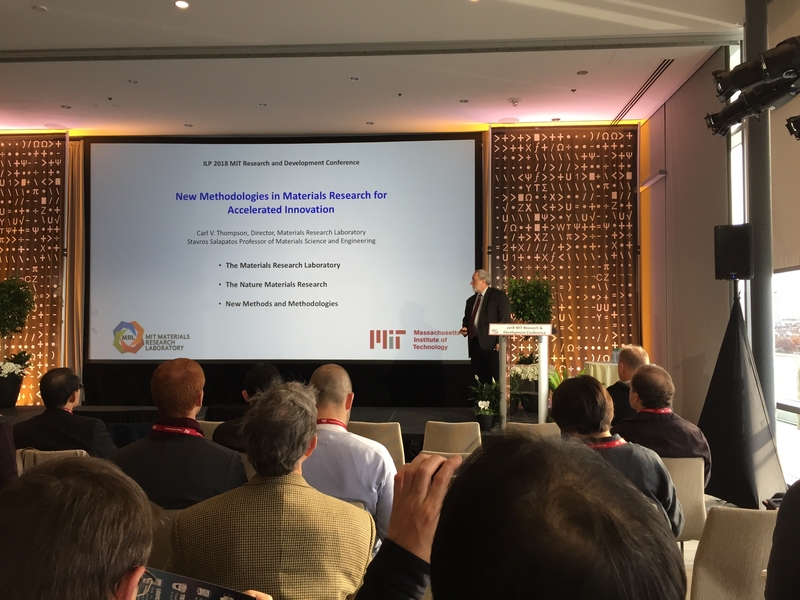
An era of rapid evolution of structures and devices driven by new capabilities in machine learning, nanoscale experiments, and economic modeling is unfolding, MIT materials researchers revealed during the annual Industrial Liaison Program (ILP) Research and Development Conference.
Pointing to progress in areas as diverse as biomedical devices, computing, and energy, Carl Thompson, director of the MIT Materials Research Laboratory and the Stavros Salapatas Professor of Materials Science and Engineering, noted the convergence of advances in nanoscale imaging and computerized prediction of materials structure and behavior with analysis of the likelihood of success in the marketplace.
A longstanding problem with green energy sources, including solar and wind, is their power production varies widely and is often mismatched to demand. Thompson noted the work of Jessika Trancik, an associate professor of energy studies who has identified the economic value of various energy storage methods based on their relative costs. These methods include compressed air, pumped water, and vanadium-based flow batteries, in addition to traditional cell-type batteries such as nickel-cadmium, lithium ion and sodium-sulfur combinations. These insights can guide the focus of research.
Flow battery trade-offs
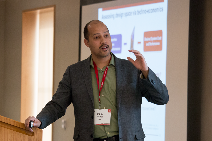
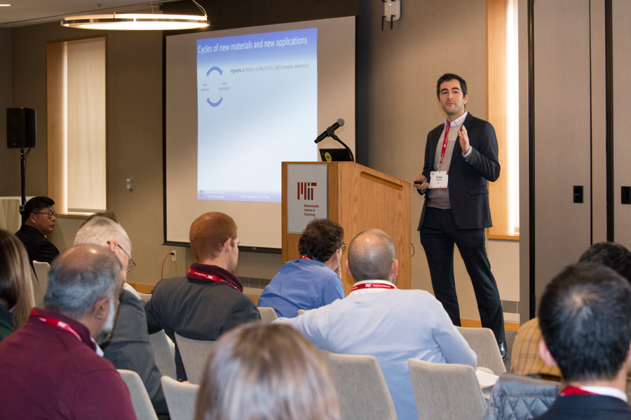
Associate professor of chemical engineering Fikile Brushett reported his progress on redox-flow batteries for grid-level electric power storage. His lab combines economic modeling with electrochemical engineering to develop better cell designs and prototypes. For the electric grid, price and lifetime are paramount, Brushett said.
Redox-flow batteries are rechargeable electrochemical devices where charge storage materials, such as vanadium, are dissolved in liquid electrolytes that are housed in tanks. To store and release power, the redox active electrolytes are pumped to a separate reactor where they undergo reversible oxidation and reduction reactions on the surface of porous carbon electrodes. Compared to enclosed batteries, this configuration offers several important advantages including long lifetimes and independent scaling of power and energy. “If you want more energy, you buy another tank,” he said.
The trade-off with these flow batteries is that current active materials, such as vanadium, are relatively expensive, meaning that system costs are high. Energy density is relatively low, meaning they are much bigger than lithium-ion batteries of comparable power. But for grid storage energy density is not at a premium, he noted.
Brushett is studying water-based chemistries with the hope of creating significantly cheaper flow batteries. One possibility is incorporating organic chemicals such as anthraquinone into the process.
“I see a lot of opportunity for scientific learning,” he said.
Appetite for electrons
Rafael Jaramillo, an assistant professor of materials science and engineering, is working to harness elements from the chalcogen group of the periodic table for solar and photonics devices. These elements — oxygen, sulfur, selenium, and tellurium — have a large variation in their appetite for electrons.
“It means they give you the biggest space of electronic materials functionality. So chalcogenides give you dielectrics, they give you semiconductors, and they give you semi-metals,” Jaramillo said. “So for somebody who is interested in electronic device technology, this is a great playground.”
Materials based on these chalcogenides change their atomic structure in response to light, and this reversible structural change holds promise for new devices suitable for integrated photonics and photovoltaics, Jaramillo said. One particular alloy of germanium, antimony, and tellurium (Ge-Sb-Te, or GST) undergoes a desirable structural change, which changes its optical property in the infrared light range, but suffers from fatigue, which produces cracks in the material.
Jaramillo is working on extremely thin metal alloys that can undergo this structural change without breaking down. This work, which is supported by the Office of Naval Research, involves computerized quantum mechanical calculations of the expected optical properties of these materials in different structural phases and then verifying the predictions experimentally.
In other realms, Jaramillo is working on chalcogenide perovskite thin films for solar cells, and is proposing a method known as tape casting to produce coatings for infrared optics.
Chip-scale chemical sensors
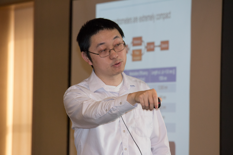
Juejun “JJ” Hu, associate professor of materials science and engineering, spoke about his new design for computer chip-sized spectrometers, devices that identify chemicals based on their response to light and that are also used to monitor optical networks. Typical benchtop spectrometers are the size of a desktop computer printer.
Hu and colleagues designed a spectrometer that acquires high-resolution spectra using a digital Fourier transformation technique in a chip-sized device. The system employs electronic optical switches instead of mirrors. A library of wavelengths of light associated with individual chemicals provide highly specific identification, making spectrometers ideal for sensing in complex environments, Hu said.
The proof-of-concept spectrometer operates in the standard communication wavelength range of 1,550 nanometers to 1,570 nanometers, which is in the infrared range. “In all cases, we were able to reproduce spectrum with very high fidelity,” Hu said.
Significantly, the more of these optical switches that are added to the setup, the higher the spectral clarity becomes, and the device performance scales exponentially with the number of switches. One possible use of these tiny chips is in sensors to detect leaks on natural gas pipelines. Hu estimates such a system could pay for itself in three years and then save $5 billion over 10 years.
Needle in a haystack
Rafael Gomez-Bombarelli, the Toyota Assistant Professor in Materials Processing, uses a process called high-throughput virtual screening. He uses machine learning to blend data from first principles calculations with data from experiments for discovering and engineering new molecules and materials for applications such as organic LEDs, photodiodes, and aqueous redox flow batteries. The process, he says, is “essentially looking for the needle in the haystack in material discovery.”
“We use our theoretical predictions, throw in chemical structure and we predict experimental properties,” Gomez-Bombarelli said. These include observable properties such as color emission and color absorption or battery efficiency, but computer simulations can often predict expected properties without the need for physical experiments.
One twist to this strategy is using numbers to represent molecules in a continuous, reversible way. “This allows us to optimize complex chemicals just like we optimize numbers, and then decode the optimal solution back to a chemical structure,” he said. “We were able to rediscover a lot of molecules that somebody has created already, as well as completely novel efficient compounds.”
Gomez-Bombarelli is applying these tools to discover better chemical compositions for peptide-based drug delivery; organic molecules for use as electrolytes in water-based redox flow batteries; polymers for photodiodes and lithium-ion batteries; or zeolites for catalyzing chemical reactions.
Talkative fibers
Yoel Fink, CEO of Advanced Functional Fabrics of America (AFFOA), described the accelerated pace of discovery in advanced fibers and fabrics at the non-profit manufacturing institute, which is a partnership of more than 75 companies and two-dozen academic institutions, state and federal agencies and private industry.
“At AFFOA, years are 90 days long,” Fink said. Each three-month research period, which focuses on a specific goal outlined in AFFOA’s roadmap, is broken up into five or six two-week long sprints.
AFFOA is developing fibers where chip and power technologies are incorporated into the fiber material itself to deliver fibers with ever increasing functionality — a Moore’s Law for fibers. AFFOA then works with industry to create fabrics that can see, hear, sense, communicate, store and convert energy, regulate temperature, monitor health, or change color. The partnership aims to create new markets for advanced fabrics where these materials provide a platform for delivering high value added services, which the company calls “fabrics as a service.”
Fink described AFFOA’s advanced fabric startup program that matches entrepreneurs with technology and provides them with access to large scale prototypes and market facing companies.
As an example of an advanced fabric, the ILP and AFFOA partnered to provide a programmable backpack to every ILP R&D conference attendee. The backpack communicates content that the owner defines through the AFFOA Looks app and fabric communications system. The backpacks were designed to enhance in-person networking and sharing connections in conferences and other events.
Fink, who is a professor of materials science and electrical engineering, demonstrated a transparent fiber with semiconductor chips in it that can survive underwater, as well as a soft fabric with communications capabilities.
AFFOA is currently developing a range of products working with Teufelberger, an Austria-based global firm with rope-making operations in Fall River, Massachusetts, to pioneer the use of rope as a communication device. For example, smart rope could inform climbers about the safety of ropes on a climb, Fink said. Smart fibers could also help self-driving cars to identify bicycle riders and athletes to connect with fans, he suggested.
The two-day ILP Research and Development Conference also addressed MIT’s innovation ecosystem, nanotechnology in life sciences, and the future of design, with additional speakers from MIT Lincoln Laboratory.
The Materials Research Laboratory partners with ILP and MIT.nano to engage with industry and promote interdisciplinary research.