The 2018 MIT Materials Research Laboratory (MRL) Materials Day Symposium, highlighting advances in materials science and engineering, took place in Kresge Auditorium on Oct. 10.
Among the latest advances shared: Powerful new combinations of X-rays, electrical probes, and analytical computing that are yielding insights into problems as diverse as fatigue in steel and stability in solar cells.
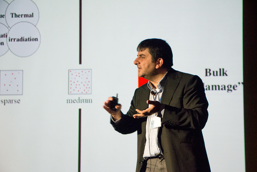
“Fatigue in steel is a major issue; you don’t see any changes in the shape of your material, and suddenly it fails," MIT Assistant Professor C. Cem Taşan said at the event. “We are putting a lot of effort in maintenance and safety, yet still we have devastating accidents,” he said, recalling the airline incident in April 2018 when a jet engine turbine blade broke apart and shrapnel from the engine broke a plane window fatally injuring a passenger.
“The airline company basically said that component passed all the maintenance requirements. So it was checked, and they couldn’t see any kind of fatigue cracks in it,” Taşan, the Thomas B. King Career Development Professor of Metallurgy, explained. Taşan is developing new steel and other metal alloys that are safer, stronger and lighter than those currently available.
Failure in metals is a complex mix of cracks and other changes in the microstructure caused by temperature, bending, stretching, compression and other forces, but most can survive at most one of these impacts before unleashing a cascade of subtle changes that ultimately result in failure.
Design for repair
Taşan outlined progress on a vanadium-based alloy that changes back to its original state when stress is taken away, and a new type of steel that can be transformed back to its original state when heat is applied. Stress tests to measure fatigue in Taşan’s new steel showed improvement over other steels.
Underlying these findings are new nanoscale experimental techniques that Taşan employs to identify the multiple causes of failure in metal alloys. Taşan combines energy-dispersive X-ray spectroscopy and scanning electron and transmission electron microscopes to capture data on tension, bending, compression or nanoindentation of materials. These type of microscopic measurements are called in situ techniques.
Another technique studies how a metal alloy absorbs hydrogen and its effect on the metal. For example, Taşan played movies that show how plastic strain is accommodated to two phases in a high-entropy alloy.
“These techniques allow us to see how the failure process is taking place, and we use these techniques to understand the mechanism of these failure modes and potentially repair mechanisms. Finally, we use this understanding to design new alloys that utilize these mechanisms,” Taşan said. “You are trying to design a mechanism that can be used by the material over and over and over again to deal with the same type of crack that it is facing.”
Taşan’s investigations revealed three different types of crack closure mechanisms in steel: plasticity, phase transformation and crack-surface roughness. “If I want to activate all of these crack closure mechanisms, what I need to do is design a microstructure that is metastable, nano-laminate(d) and multi-phase at same time,” he said. He said the new steel alloy successfully combines all three characteristics.
Materials Research Laboratory Director Carl V. Thompson noted that how a material is made determines its structure and its properties. These properties include mechanical, electrical, optical, magnetic and many other properties. Materials science and engineering encompasses an entire cycle from designing methods for making materials through analyzing their structure and properties, to evaluating how they perform. “Ultimately most people go through this process to make materials that perform in either a new way or in a better way for systems like automobiles, your cell phone, or medical equipment,” Thompson said.
Engineering perovskite solar cells
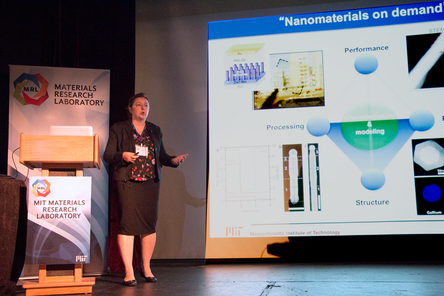
Silvija Gradečak, professor in the Department of Materials Science and Engineering, addressed the promise and the problems of perovskite solar cells. Hybrid organic-inorganic perovskites, such as methyl ammonium lead iodide, are a class of materials that are named after their crystal structure. “They are potentially lightweight, flexible and inexpensive as photovoltaic devices,” Gradečak said.
However, perovskite solar devices tend to be unstable in water, oxygen exposure, UV irradiation, and under-voltage biasing. As many of these changes are dynamic and happen at nanoscale, understanding the structure of these materials can be complemented with information from electrical currents. “By using the electron beam, we can mimic the condition of the electron current within the device,” she said.
Gradečak uses a technique called cathodoluminescence to probe these perovskite materials. “Our cathodoluminescence setup is unique because it enables so-called hyperspectral imaging. It means that the full optical signal is detected in each point of the complementary structural image. As the beam interacts with the sample, we are detecting light, and we do this as the electron beam moves across the sample. That is specifically important for samples that are unstable as they are irradiated with the electron beam,” she says.
This technique revealed that perovskite material examined under an electron microscope while applying a voltage to the sample for one minute resulted in a dramatic current increase in the material. “That also corresponds to the I/V [current/voltage] measurements outside of the scanning electron microscope that we performed,” she said. When the voltage bias is removed, the sample relaxes back to its initial state.
“What we think is really happening is that by biasing, there are ions that are moving and they agglomerate at the edges of the sample or at the grain boundaries, and after you remove the bias, they will relax back,” Gradečak said.
Work in Gradečak’s group by Olivia Hentz PhD ’18 combined photoluminescence data with Monte Carlo simulations to extract mobility of the defects that are moving. “More interesting, and how we can apply this method, is to understand how the material’s properties are influenced by synthesis. If you synthesize the material and you change, for example, the grain size, we can think about whether these ions that are moving will have different mobilities inside of the grain versus along the grain boundaries,” Gradečak said.
Hentz found that the mobility at the grain boundaries is 1,500 times faster than in the bulk. “The ions do move in the material, they move under the biasing conditions and that mobility is very different inside of the grain and along the grain boundaries,” Gradečak said. “By engineering the material and engineering the grain size, one can influence by how much the material will be influenced during the device operation. And this result correlates with the fact that single crystalline perovskite materials are significantly more stable than polycrystalline ones.”
Transformative new tools
In the keynote address, BP Amoco Chemical Company Senior Research Chemist Matthew Kulzick detailed new X-ray technologies and sample chambers that are yielding insights into fighting metal corrosion, improving catalytic reactions and more. “The current evolution of tools is spectacular,” he said, noting the stunning images at 20-nanometer scale showing highly localized composition of materials.
MIT Nuclear Reactor Lab Director David E. Moncton discussed advances in X-ray tubes, noting that current versions of small scale X-ray tubes are about 100 times better than those of 100 years ago. X-ray source brilliance is increasing at two times Moore’s Law, which predicted the exponential growth of transistors in silicon chips, he noted.
Still Synchroton sources such as the Advanced Photon Source, a national user facility at Argonne National Laboratory, offer beam brilliance that is 12 orders of magnitude higher than X-ray tubes. “Advanced X-ray capability is the most important missing probe of matter at nano centers and materials research labs that are not located at synchrotron facilities,” he said.
Compact X-ray free-electron laser devices hold the promise of bringing synchrotron-like examination capabilities to campus research labs, Moncton said. Moncton, who was the founding director of the Advanced Photon Source, is collaborating with Associate Professor William S. Graves at Arizona State University, which is home to world’s first compact X-ray free-electron laser (CXFEL).
“The emittance is very similar to a synchrotron source,” Moncton said. “If you built a compact X-ray FEL on this compact source platform, it would outperform today’s synchrotron facilities by a number of orders of magnitude.”
X-ray phase contrast imaging has also advanced microscopy, Moncton said, displaying an image showing air bubbles in the lungs of a fruit fly. Pump-probe techniques enable studies of biological proteins performing bio-chemical processes in real time.
“Having a local synchrotron-like source would be revolutionary,” Moncton said.
Less damaging microscope
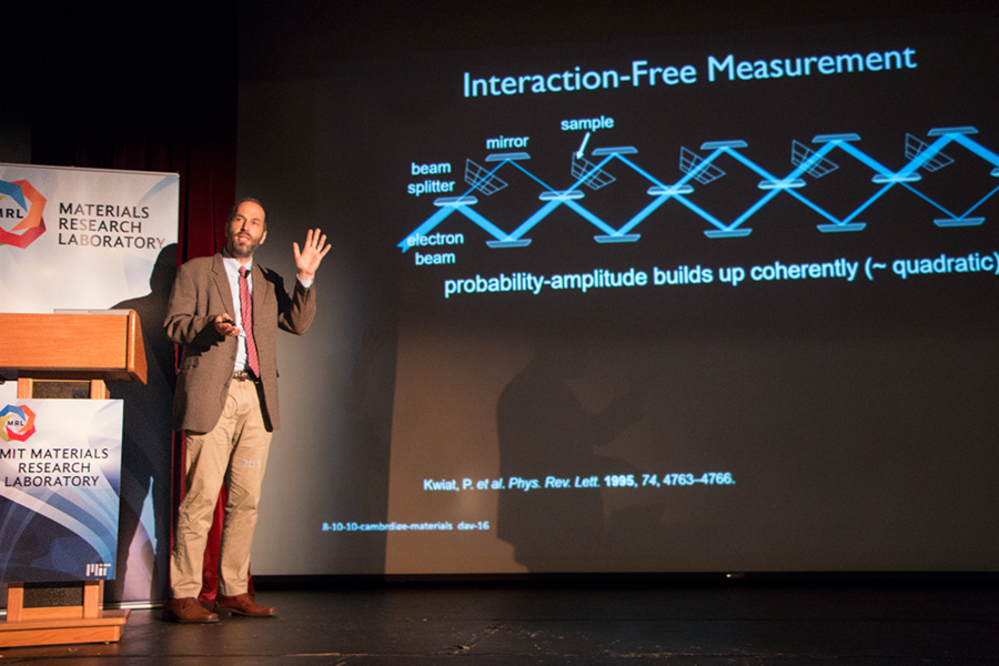
MIT professor of electrical engineering Karl Berggren described his efforts to develop a new type of electron microscope based on the quantum character of electrons to improve microscopy. One of the goals is to reduce radiation damage to biological samples from imaging them.
With support from the Gordon and Betty Moore Foundation, Berggren is collaborating on this research with professor of physics Mark Kasevich at Stanford University, professor of physics Peter Hommelhoff at the Friedrich Alexander University, Erlangen-Nürnberg, in Germany, and professor of physics Pieter Kruit at the Technical University of Delft in the Netherlands. “What we’d like to do is basically try to take advantage of the counter-intuitive quantum properties of electrons,” Berggren said.
In one approach, he employs a series of electron beam splitters and mirrors to improve the performance of scanning electron microscopes. “What we’re doing now is essentially making a test bed by which we can develop all the electron optics to try to put together a machine,” Berggren said. Along the way, his group has developed a microscope that lets you image the top and bottom of a sample at the same time.
“We know that electrons at high voltage will pass through many samples with interacting with just a small phase shift,” he said. “In fact, we want to work in that limit for imaging bio molecules.” The right combination of beam splitters could reduce electron-induced damage to the sample by 100 times, he said.
Nanowire self-assembly
Frances M. Ross, formerly of the Research Division at the IBM T. J. Watson Research Center and a new arrival at the Department of Materials Science and Engineering this academic year, described her observations of nanowire growth in an electron microscope. This vapor-liquid-solid process was first described in 1964, but the atomic-level details of how the nanowires grow could not be observed until recent improvements in electron microscopy technique.
Showing a movie of a silicon nanowire growing from a gold-silicon catalyst droplet, Ross said, “To grow these silicon nanowires, we just put gold on silicon and heat it up. The gold and silicon automatically form droplets, in the same way that water forms droplets on a sheet of glass.” When additional silicon is then supplied, the droplets act as a catalyst and a silicon nanowire grows from each droplet. “Nanowire growth illustrates the fact that we can get a self-assembly process that is intrinsically very simple to form a structure that can be quite complex,” Ross explained. “You can see features like the atomic level structure of the nanowire and catalyst, the effect of temperature and gas environment, and even the dynamics of the growth interface and how the catalyst really works.” The silicon nanowire grows in little jumps despite a steady flow of source material, she noted, providing detailed information on the pathways by which the atoms assemble into the nanowire.
Adding nickel to this process resulted in a nickel disilicide particle embedded in the silicon nanowire — a quantum dot. “You almost expect to see unexpected things because the movies capture every point along the way as the material evolves,” Ross said. “In situ microscopy is really the only way to get these type of detailed relations between the structure, the properties, and even the catalytic activity of individual nanoscale objects.”
“We’re in a very exciting time for electron microscopy, where advances in instrumentation are helping us understand materials growth at the atomic scale,” Ross said.
Uncovering crystal structure
James LeBeau, visiting professor of materials science and engineering, explained that scanning transmission electron microscopy provides direct imaging of atomic structure using an extremely small (less than 1x10⁻¹⁰m) electron probe. LeBeau uses the scanning transmission electron microscope to develop and apply new ways to characterize atomic structure of materials to understand their properties. Further, he is applying machine learning to control the microscope, using an approach similar to that used to enable self-driving cars to recognize signs and lane lines.
Beyond imaging, “we can also acquire a full chemical spectrum at every single point in our dataset. This allows us to not only directly determine which atoms are in the material, but their bonding configuration as well,” LeBeau explained. He displayed an image showing lanthanum atoms sharing a sub-lattice with strontium and aluminum sharing a sub-lattice with tantalum. “These datasets become directly interpretable. You see the chemistry,” he said.
“We can even use this data to measure the atomic scale electric field,” LeBeau added, showing an image in which the color represents the electrostatic field vector and the intensity of the color represents its magnitude. LeBeau also was able to use these techniques to uncover the particular crystal structure of ferroelectric hafnium dioxide. The atomic scale insights are critical as hafnium dioxide is compatible with silicon processing technology, which will pave the way for new memory applications. “By combining different types of data, we can explain the origin or ferroelectricity in these films and really rule out alternative explanations,” he said.
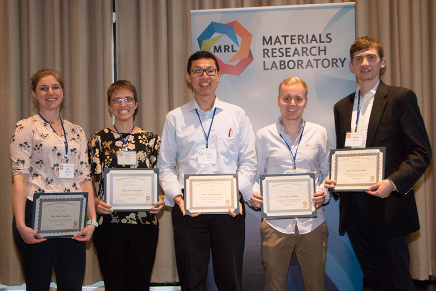
Twenty graduate students and postdocs gave two-minute previews during the Materials Day Symposium, which was immediately followed by a poster session. In all, 60 presented research posters in La Sala de Puerto. The winning presenters were graduate students Vera Schroeder, Rachel C. Kurchin, Gerald J. Wang and Philipp Simons, and postdoc Mikhail Y. Shalaginov.