Photonics — the science of guiding and manipulating light — enables applications ranging from telecommunications, artificial intelligence, and quantum computing to medical imaging, lidar, and augmented reality displays. But despite the importance of this growing field, the nation faces a shortage of photonics and electronics technicians and engineers.
The Lab for Education and Application Prototypes (LEAP), located on the fifth floor of MIT.nano, is a research laboratory that also functions as a hands-on classroom for learning how to package electronic and photonic chips. This open-access facility was the first in what is now a network of five labs supporting innovation in advanced manufacturing across Massachusetts.
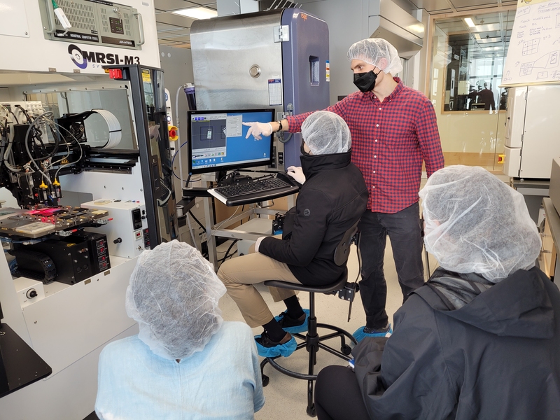
The MIT LEAP is outfitted with tools for electronic-photonic packaging including a die bonder, wire bonders, an X-ray inspection system, a large area microscope, a plasma treatment machine, and a reflow oven for soldering applications — but it’s not just about the tools, says Anu Agarwal, principal research scientist in the Materials Research Laboratory and leader of the LEAP at MIT.
“LEAP is about what we are doing with the tools. We are educating students from all over — MIT, other four-year institutions, community colleges, and industry employees — to understand the technology and develop prototypes to advance manufacturing and strengthen the future electronics and photonics workforce,” she says.
The history behind MIT’s LEAP
The LEAP network began in 2015 as a result of a federal initiative to revitalize manufacturing in the United States. The national manufacturing institute AIM Photonics and the Massachusetts Manufacturing Innovation Initiative, a state grant program managed by the MassTech Collaborative, allocated a combined $11.3 million to build labs across Massachusetts. Under the leadership of MIT Microphotonics Center Director Lionel Kimerling, professor of materials science and engineering, MIT.nano Associate Director Brian Anthony, principal research scientist in mechanical engineering and Microsystems Technology Laboratories Associate Director for Computation and CAD Duane Boning, the Clarence J. LeBel Professor in Electrical Engineering, $1 million was awarded for the first LEAP to be established at MIT.
The LEAP aims to accomplish four main tasks — teach integrated photonics manufacturing practice; provide small and medium enterprise (SME) technician training and certification; encourage startup and SME engagement in tool, process, and application upgrades; and support AIM Photonics multi-project wafer and Test, Assembly, and Packaging hubs.
To meet these goals, faculty and staff from the MIT Initiative for Knowledge and Innovation in Manufacturing (IKIM), led by Kimerling, offer blended learning boot camps that include a hands-on component through the AIM Photonics Academy, a branch of the national AIM Photonics Institute located at MIT, to train learners in integrated photonics testing and packaging. The LEAP is used by undergraduates to study packaging science, by graduate students to conduct research in packaging innovations, and by local industry for prototyping. In January 2022, the Microphotonics Center and IKIM launched an electronic-photonic packaging industry consortium, directed by Agarwal, to promote pre-competitive partnerships between academic institutions, companies, and government to develop ideas that will lead to next-generation products.
“In addition to academic institutions, it’s important to support local ventures,” says Farhad Vazehgoo, MassTech director for advanced technology programs and workforce development. “By introducing SMEs such as Pendar Technologies and Sheaumann Laser to MassTech’s funding opportunities, MIT’s LEAP is helping us lay the groundwork for new photonics companies across the state, which will enable the creation of high-tech, integrated photonics manufacturing jobs.”
Expanding across Massachusetts
Since its origins at MIT, the LEAP network has expanded to comprise five integrated photonics-based labs in Massachusetts, creating a geographically distributed network focused on STEM education, workforce development, and industry/academic collaboration.
The labs are not all the same. While the MIT LEAP focuses on packaging, the LEAP at Worcester Polytechnic Institute/Quinsigamond Community College specializes in biomedical photonics applications; the LEAP at Stonehill College is a materials characterization and high-speed device testing hub; and Bridgewater State University’s LEAP focuses on mid-infrared lasers and quantum-device-based photonics. The fifth LEAP, established at Western New England University/Convergent Photonics in 2020, is focused on high-power lasers.
Having these different specialties creates a statewide ecosystem of varying expertise with a common goal to train the manufacturing workforce across the photonics supply chain. The facilities are strategically located near community colleges, bringing together different hierarchy of academic institutions as well as different students. “Not everyone wants to get a PhD,” says Agarwal, stressing the importance of reaching all types of learners and in various stages of their careers.
Hands-on photonics education
To support laboratory training, the LEAPs use hands-on photonics education kits created by the AIM Photonics Institute. The kits include chips designed by Rochester Institute of Technology Professor Stefan Preble, University of Rochester Assistant Professor Jaime Cardenas, and Boston University Associate Professor Miloš Popović, and fabricated at the AIM Photonics foundry under the leadership of Kimerling. These chips consist of passive and active photonic integrated circuit devices that can be tested by grating coupling or edge coupling from a fiber to the chip. The kits also include detailed laboratory workbooks for instructors and students.
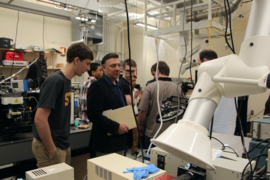
After a pause on boot camps due to Covid-19, Agarwal says, LEAP is returning to regular activities for individuals from industry, academia, and government. On March 22-24, the MIT and Bridgewater State University LEAPs offered the first joint Integrated Photonics Bootcamp to train engineers on photonic and electronic device packaging and testing. At MIT.nano, learners bonded surface-mounted light-emitting diodes on printed circuit boards using a high-speed pick-and-place tool; performed solder reflow and X-ray imaging; and programmed their sensors to illuminate the diodes. Device testing was performed at the Bridgewater State University LEAP.
Those who cannot join LEAP workshops in-person can take advantage of AIM Photonics Academy’s online courses hosted by the U.S. Department of Defense’s Manufacturing USA. The IKIM is also developing a series of virtual-reality (VR)-based training simulations of tools led by MIT research scientist Erik Verlage and AIM Photonics Academy Education Director Sajan Saini using LEAP simulation servers in MIT Department of Electrical Engineering and Computer Science Professor Duane Boning’s laboratory. At the recent bootcamp, attendees tested these desktop VR simulations to demonstrate how they can minimize orientation time at the physical tool, reduce tool breakage due to newcomer mistakes, and enable remote, self-paced training.
The MIT team continues to collaborate with the other four LEAPs to leverage different tool capabilities. “The LEAP network strives to be a blended learning STEM education and workforce training model for the rest of the country,” says Agarwal. “From ideas to actual labs, to educating the current and next generations, we aim to build interest and engagement in STEM,” adds Kimerling.