
MIT researchers have, for the first time, fabricated a diamond-based quantum sensor on a silicon chip. The advance could pave the way toward low-cost, scalable hardware for quantum computing, sensing, and communication.
“Nitrogen-vacancy (NV) centers” in diamonds are defects with electrons that can be manipulated by light and microwaves. In response, they emit colored photons that carry quantum information about surrounding magnetic and electric fields, which can be used for biosensing, neuroimaging, object detection, and other sensing applications. But traditional NV-based quantum sensors are about the size of a kitchen table, with expensive, discrete components that limit practicality and scalability.
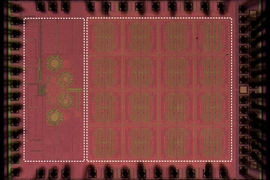
In a paper published in Nature Electronics, the researchers found a way to integrate all those bulky components — including a microwave generator, optical filter, and photodetector — onto a millimeter-scale package, using traditional semiconductor fabrication techniques. Notably, the sensor operates at room temperature with capabilities for sensing the direction and magnitude of magnetic fields.
The researchers demonstrated the sensor’s use for magnetometry, meaning they were able to measure atomic-scale shifts in the frequency due to surrounding magnetic fields, which could contain information about the environment. With further refining, the sensor could have a range of applications, from mapping electrical impulses in the brain to detecting objects, even without a line of sight.
“It’s very difficult to block magnetic fields, so that’s a huge advantage for quantum sensors,” says co-author Christopher Foy, a graduate student in the Department of Electrical Engineering and Computer Science (EECS). “If there’s a vehicle traveling in, say, an underground tunnel below you, you’d be able to detect it even if you don’t see it there.”
Joining Foy on the paper are: Mohamed Ibrahim, a graduate student in EECS; Donggyu Kim PhD ’19; Matthew E. Trusheim, a postdoc in EECS; Ruonan Han, an associate professor in EECS and head of the Terahertz Integrated Electronics Group, which is part of MIT's Microsystems Technology Laboratories (MTL); and Dirk Englund, an MIT associate professor of electrical engineering and computer science, a researcher in Research Laboratory of Electronics (RLE), and head of the Quantum Photonics Laboratory.
Shrinking and stacking
NV centers in diamonds occur where carbon atoms in two adjacent places in the lattice structure are missing — one atom is replaced by a nitrogen atom, and the other space is an empty “vacancy.” That leaves missing bonds in the structure, where the electrons are extremely sensitive to tiny variations in electrical, magnetic, and optical characteristics in the surrounding environment.
The NV center essentially functions as an atom, with a nucleus and surrounding electrons. It also has photoluminescent properties, meaning it absorbs and emits colored photons. Sweeping microwaves across the center can make it change states — positive, neutral, and negative — which in turn changes the spin of its electrons. Then, it emits different amounts of red photons, depending on the spin.
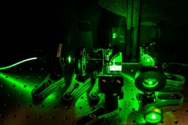
A technique, called optically detected magnetic resonance (ODMR), measures how many photons are emitted by interacting with the surrounding magnetic field. That interaction produces further, quantifiable information about the field. For all of that to work, traditional sensors require bulky components, including a mounted laser, power supply, microwave generator, conductors to route the light and microwaves, an optical filter and sensor, and a readout component.
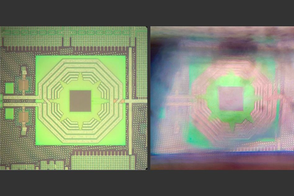
The researchers instead developed a novel chip architecture that positions and stacks tiny, inexpensive components in a certain way using standard complementary metal-oxide-semiconductor (CMOS) technology, so they function like those components. “CMOS technologies enable very complex 3-D structures on a chip,” Ibrahim says. “We can have a complete system on the chip, and we only need a piece of diamond and green light source on top. But that can be a regular chip-scale LED.”
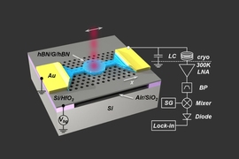
NV centers within a diamond slab are positioned in a “sensing area” of the chip. A small green pump laser excites the NV centers, while a nanowire placed close to the NV centers generates sweeping microwaves in response to current. Basically, the light and microwave work together to make the NV centers emit a different amount of red photons — with the difference being the target signal for readout in the researchers’ experiments.
Below the NV centers is a photodiode, designed to eliminate noise and measure the photons. In between the diamond and photodiode is a metal grating that acts as a filter that absorbs the green laser photons while allowing the red photons to reach the photodiode. In short, this enables an on-chip ODMR device, which measures resonance frequency shifts with the red photons that carry information about the surrounding magnetic field.
But how can one chip do the work of a large machine? A key trick is simply moving the conducting wire, which produces the microwaves, at an optimal distance from the NV centers. Even if the chip is very small, this precise distance enables the wire current to generate enough magnetic field to manipulate the electrons. The tight integration and codesign of the microwave conducting wires and generation circuitry also help. In their paper, the researchers were able to generate enough magnetic field to enable practical applications in object detection.
Only the beginning
In another paper presented earlier this year at the International Solid-State Circuits Conference, the researchers describe a second-generation sensor that makes various improvements on this design to achieve 100-fold greater sensitivity. Next, the researchers say they have a “roadmap” for how to increase sensitivity by 1,000 times. That basically involves scaling up the chip to increase the density of the NV centers, which determines sensitivity.
If they do, the sensor could be used even in neuroimaging applications. That means putting the sensor near neurons, where it can detect the intensity and direction of firing neurons. That could help researchers map connections between neurons and see which neurons trigger each other. Other future applications including a GPS replacement for vehicles and airplanes. Because the magnetic field on Earth has been mapped so well, quantum sensors can serve as extremely precise compasses, even in GPS-denied environments.
“We’re only at the beginning of what we can accomplish,” Han says. “It’s a long journey, but we already have two milestones on the track, with the first-and second-generation sensors. We plan to go from sensing to communication to computing. We know the way forward and we know how to get there.”
“I am enthusiastic about this quantum sensor technology and foresee major impact in several fields,” says Ron Walsworth, a senior lecturer at Harvard University whose group develops high-resolution magnetometry tools using NV centers.
“They have taken a key step in the integration of quantum-diamond sensors with CMOS technology, including on-chip microwave generation and delivery, as well as on-chip filtering and detection of the information-carrying fluorescent light from the quantum defects in diamond. The resulting unit is compact and relatively low-power. Next steps will be to further enhance the sensitivity and bandwidth of the quantum diamond sensor [and] integrate the CMOS-diamond sensor with wide-ranging applications, including chemical analysis, NMR spectroscopy, and materials characterization.”