On a recent evening, Cathrin Stickney stood marveling at the stillness of the custom-designed imaging suites in the underground level of MIT.nano — the environmentally quietest space on campus. Laudably ultra-low vibrations, ultra-low electromagnetic interference, and acoustically silent. All in a building that, like most of the rest of MIT, sits on a century-old landfill built on swampland.
“It’s more than difficult to pull that off. It’s architecturally amazing,” Stickney, a successful entrepreneur and former architect, said. Equipped with a neon safety vest and clear safety glasses, Stickney was on site to learn more about a building that embodies one of the largest research investments in MIT history.
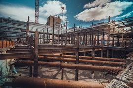
The leaders of MIT.nano pulled out all the stops during the first-ever tour of the 214,000 gross-square-foot research facility taking shape in the heart of MIT campus, just steps from the Infinite Corridor. The tightly choreographed public viewing involved safely navigating 60 guests, mostly members of the MIT Corporation, through what is still an active construction site.
Nanoscience and nanotechnology are driving some of the most important innovations today, in health care, energy, computing — almost every field of engineering and science. A facility that allows MIT faculty and students to play a role in these coming changes is of the Institute’s highest priority, says President L. Rafael Reif, who was along for the tour. As he has said: “Even big problems have answers if you have your hands on the right tools.”
As the tour group convened in a conference room near where they would access the site, the project’s faculty lead, Vladimir Bulović, fine-tuned that sentiment. “The toolset we need to bring forward the next generation of ideas is a nano toolset,” and with those words Bulović and his team launched the first public showing of MIT.nano.
The sneak peek
Starting in the MIT.nano subterranean level, Stickney and husband Mark Gorenberg ‘76, a venture capitalist, took in the cavernous space. The imaging suites are set on what Dennis Grimard, the building’s operations director, calls “The Inertia Slab” — a structure that complements the location of MIT.nano, and makes it the quietest spot on campus. The slab is a block made of 3.2 million pounds of concrete poured onto 400,000 pounds of epoxy-coated rebar. Its creation required approximately more than 100 cement trucks operated continuously in a single day from 4 a.m. to 4 p.m.
With hands clasped, the couple listened attentively as Thomas Schwartz, a biology professor, spoke about the scope of research MIT.nano will enable. The extreme shielding from environmental noise, he said, will satisfy the challenging low-vibration demands of high-end electron microscopes, particularly those for biological imaging. His delight was palpable. “These new microscopes will allow us to visualize large protein complexes at atomic resolution, and to observe thin sections of entire cells in nanometer precision,” said Schwartz, the Boris Magasanik Professor of Biology. “This truly represents a quantum leap for structural and cell biology!”
On the construction elevator, jolting from the basement to the first floor, Stickney said: “The massive amount of effort put into all of this is stunning.” Shouting above the wind, Gorenberg agreed. It makes sense from an investment standpoint, he remarked. “Nanotechnology cuts across all disciplines, so it’s going to be vital to everyone.”
The clean rooms
The hoist clanged to a stop, and the group exited to check out state-of-the-art clean rooms. Waiting for them was Luis Velásquez-García, a principal research scientist in the Microsystems Technology Laboratories, and an expert in micro- and nanofabrication technologies. Outfitted in a white jumpsuit, he quickly launched into a description of how MIT.nano will open new worlds for researchers. The clean room will be like a hive, he said, bustling with people working together to make breakthroughs in nanotechnology. It will enable: devices that can produce X-rays for medical imaging, nanosatellite propulsion, and plasma diagnostics. He described a future in which nanotechnology-enabled materials dramatically change 3-D-printing technology.
Tour guests checked out the clean rooms on the third level, too, where sunlight pours through glass in hallways that overlook the MIT dome and new courtyard below. Krystyn Van Vliet, a professor of materials science and engineering and biological engineering, described how clean rooms will provide a precisely controlled environment with low levels of dust, airborne microbes, aerosol particles, chemical vapors, and anything else that can get in the way of their work. Van Vliet, the Michael (1949) and Sonja Koerner Professor of Materials Science and Engineering, studies material behavior at the interface of mechanics, chemistry, physics, and biology. She informed tour guests that the facility will connect MIT experts in materials synthesis, characterization, and teaching for a range of applications, and build on the inspiration of interdisciplinary collaborators such as the late Institute Professor Emerita of Physics and Electrical Engineering and Computer Science Mildred Dresselhaus.
Van Vliet, the director of manufacturing innovation for the MIT Innovation Initiative, also said MIT.nano is poised to support an innovation community that will help usher in next-generation manufacturing processes and training approaches for production of electronics, photonics, fibers, and biopharmaceuticals. For instance, the facility will benefit academic and industry partnerships for MIT researchers who participate in Manufacturing USA Institutes, a network of public-private partnerships between government, industry, and academia focused on de-risking and prototyping new manufacturing capabilities to speed adoption by U.S. manufacturers.
Throughout the building, MIT faculty were working hard to convey their excitement. Academics were situated on every level, and even the guides escorting guests through the building were impressively credentialed: Anuradha Agarwal, a principal research scientist at the Microphotonics Center who develops miniaturized chemical sensors; Polina Anikeeva, the Class of 1942 Career Development Professor in the Department of Materials Science and Engineering who stimulates brain activity using nanotechnologies; electrical engineering professors Karl Berggren, who specializes in nanofab and quantum devices, and Rajeev Ram, who develops novel photonics and electronics; and William Tisdale, the Charles and Hilda Roddey Career Development Professor in Chemical Engineering, who explores use of
colloidal quantum dots and 2-D materials in next-generation renewable energy technologies. All the stops, pulled.
A game-changer
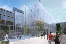
MIT.nano is designed as an invitation to the community. With 53,000 square-feet of glass on its exterior surface, the new building may be surrounded on all sides by other buildings, but it’s appearance and effect are transparency. As Grimard explains, “Typically, MIT buildings have windowed offices along the outside and labs get placed on the inside. We did just the opposite. We wanted the MIT community to see inside and have that connectivity with the space. This is everyone’s building.”
Prepared to serve more than 2,000 researchers from across campus, MIT.nano will be transformative. An interior building set in the footprint of the former Building 12, its broader visibility will rely greatly on the research collaborations forged within its walls. Those connections hold the power to reimagine MIT.
The wrap-up
The guests finished by touring the upper levels of MIT.nano. On the fifth floor, which is dedicated to prototyping maker spaces and teaching labs, presenter Brian Anthony, director of MIT’s Master of Engineering and Manufacturing Program, told guests MIT.nano will become a central resource for creating disruptive technologies. Researchers will gain the ability to distinguish and manipulate materials at the atomic scale, create devices using those materials, and develop ways of implementing those devices within larger systems. MIT.nano is not owned by any one area of MIT, he said. Or put simply, added Anthony: “MIT.nano is like an iPhone — and researchers across campus are welcome to make the apps.”
Nodding as he listened, John Chisholm ’75, SM ’76, a serial entrepreneur, commented: “You can see how many disciplines meet here,” he said. “This is the future of research and education: conventional boundaries among schools and departments are disappearing."
Chisholm and the other guests piled back into the hoist, which came to its final stop: the mechanical penthouse, where MIT.nano’s senior project manager Travis Wanat awaited. Wanat is a true believer in the promise of MIT.nano. He met with 35 labs, centers, and departments — mainly abutters to the site — to allay concerns from the start. Not an easy task when simply pouring the foundation involved the removal of 1.4 million cubic feet of dirt. Now the project, which Bulović refers to as a dream nearing reality, is finally — at least briefly — on public display. Wanat eagerly detailed the construction process and took a barrage of questions about prefabrication strategy, metrics for overall savings, the early procurement process, and more.
Satisfied with the detailed answers, the Corporation members descended by stairs to the unfinished courtyard below. They held metal handrails rather than wooden ones, warned earlier of splinters. They spoke of the building design — particularly the energy conservation strategies — with approval.
“The building is amazingly larger than any of us could have imagined,” said Gorenberg. Alan Spoon ’73, a venture capitalist, added: “The opportunity for students and researchers to be rubbing shoulders in the most productive way imaginable is mind blowing.” Trailing behind for a final look, the granddaughters of Dresselhaus, a beloved scientist, described weekly lunches during which Dresselhaus would pull them to a window from where they would observe construction progress. “She was so excited about the MIT.nano building,” said Leora Cooper. “She loved it and the future it brings.”