Doug Spreng '65 graduated with a degree in electrical engineering, and spent the next 40 years in high-tech manufacturing and marketing. He served as a general manager for Hewlett-Packard, executive vice president for 3Com, and chairman and CEO for Ubicom.
After he retired in 2006, Spreng devoted himself to supporting MIT in a variety of ways. He sits on the visiting committee of the Department of Materials Science and Engineering, and fundraises for energy research. He also serves as president of the MIT Club of Northern California and chairs the club’s energy and environment program, which brings MIT faculty to present the latest in energy research to local alumni.
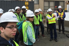
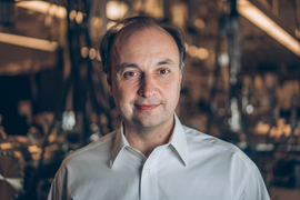
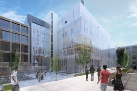
At one of these gatherings, Vladimir Bulović, the Fariborz Maseeh Chair in Emerging Technology, discussed the launch of MIT.nano, the Institute’s new nanoscale characterization and fabrication facility that Bulović will lead, and which is due to open in June 2018. Convinced of the significance of nanoscience to future technological innovations, and the impact of the new facility on those innovations, Spreng took on yet another role: MIT.nano evangelist.
Q: You started your career as digital technology began to transform the economy. Do you think nanotechnology might prove to be as revolutionary a force?
A: Whenever you have a new set of technologies or discoveries that come along, like the invention of the transistor or breaking of the genetic code, it’s impossible to know where they can go ultimately. Nanotechnology is that kind of thing; its impact is only limited by the imagination. I also have faith that if you put together a center at MIT staffed with bright people and the latest equipment, great things will happen.
Q: In what areas do you envision nanotechnology will make a significant impact?
A: Wherever materials can be used. Nanotechnology lends itself to a multiplicity of applications. It is already in use in the semiconductor industry, in photolithography. There will be major impacts in the area of renewable energy, with breakthroughs in high-efficiency materials for wind turbines and solar photovoltaics. Nanofluids can be used to improve nuclear energy efficiency, and might help with battery storage as well. Who knows, we could see wearable technology, where you embed flexible circuits in fabric. Maybe we’ll be wearing a solar collector as a shirt, generating a bit of power for our smartphones.
Companies might not yet have a clue how nanotechnology might help them. But if they’re in a business where materials define their products, it would behoove them to invest heavily in research to come up with more effective or less expensive materials. Speculative projects in nanotechnology offer the possibility of big payoffs.
Q: You have a lot of experience helping new technologies reach large-scale implementation. What’s the role of a research university in this transition?
A: These days, it’s crucial. Back when I started my career, a number of large companies such as IBM, HP, and AT&T (through Bell Labs) did most of the basic research in the U.S. The government also invested in certain areas, with an eye towards defense and sometimes in the health and life sciences. But the national labs didn’t have a brilliant track record of getting breakthrough technologies to market. Over time, government began funding university research programs, and as large companies reduced investment in their own R&D they also began linking up with research universities.
Today, university research really starts the process for new technologies to be implemented and commercialized, which is a very good thing. MIT has a big program for doing this. We need research that accomplishes something in the world, which solves real problems.
Q: If you could start over and enroll at MIT tomorrow, what would you study?
A: I’d probably major in Course 3 [materials science and engineering]. When I was in school in the early ’60s, it was called metallurgy. I like hands-on things, and I’m wowed by possibilities in materials these days. Another area I’d like to explore is biotechnology, maybe something involved with the human genome. It would be great to help solve or eliminate diseases and birth defects, and bring enormous benefits to mankind. I might also be interested in looking at ways to use genetically modified organisms for dramatically improving yields on crops, to feed the world’s growing population.
In the past 50 years technology has changed the world in stunning ways. Why expect it to slow down? We’re just scratching the surface in new areas. We’ve got decades to go in terms of discovery.