Researchers at MIT say they have carried out a theoretical analysis showing that a family of two-dimensional materials exhibits exotic quantum properties that may enable a new type of nanoscale electronics.
These materials are predicted to show a phenomenon called the quantum spin Hall (QSH) effect, and belong to a class of materials known as transition metal dichalcogenides, with layers a few atoms thick. The findings are detailed in a paper appearing this week in the journal Science, co-authored by MIT postdocs Xiaofeng Qian and Junwei Liu; assistant professor of physics Liang Fu; and Ju Li, a professor of nuclear science and engineering and materials science and engineering.
QSH materials have the unusual property of being electrical insulators in the bulk of the material, yet highly conductive on their edges. This could potentially make them a suitable material for new kinds of quantum electronic devices, many researchers believe.
But only two materials with QSH properties have been synthesized, and potential applications of these materials have been hampered by two serious drawbacks: Their bandgap, a property essential for making transistors and other electronic devices, is too small, giving a low signal-to-noise ratio; and they lack the ability to switch rapidly on and off. Now the MIT researchers say they have found ways to potentially circumvent both obstacles using 2-D materials that have been explored for other purposes.
Existing QSH materials only work at very low temperatures and under difficult conditions, Fu says, adding that “the materials we predicted to exhibit this effect are widely accessible. … The effects could be observed at relatively high temperatures.”
“What is discovered here is a true 2-D material that has this [QSH] characteristic,” Li says. “The edges are like perfect quantum wires.”
The MIT researchers say this could lead to new kinds of low-power quantum electronics, as well as spintronics devices — a kind of electronics in which the spin of electrons, rather than their electrical charge, is used to carry information.
Graphene, a two-dimensional, one-atom-thick form of carbon with unusual electrical and mechanical properties, has been the subject of much research, which has led to further research on similar 2-D materials. But until now, few researchers have examined these materials for possible QSH effects, the MIT team says. “Two-dimensional materials are a very active field for a lot of potential applications,” Qian says — and this team’s theoretical work now shows that at least six such materials do share these QSH properties.
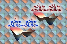
The MIT researchers studied materials known as transition metal dichalcogenides, a family of compounds made from the transition metals molybdenum or tungsten and the nonmetals tellurium, selenium, or sulfur. These compounds naturally form thin sheets, just atoms thick, that can spontaneously develop a dimerization pattern in their crystal structure. It is this lattice dimerization that produces the effects studied by the MIT team.
While the new work is theoretical, the team produced a design for a new kind of transistor based on the calculated effects. Called a topological field-effect transistor, or TFET, the design is based on a single layer of the 2-D material sandwiched by two layers of 2-D boron nitride. The researchers say such devices could be produced at very high density on a chip and have very low losses, allowing high-efficiency operation.
By applying an electric field to the material, the QSH state can be switched on and off, making possible a host of electronic and spintronic devices, they say.
In addition, this is one of the most promising known materials for possible use in quantum computers, the researchers say. Quantum computing is usually susceptible to disruption — technically, a loss of coherence — from even very small perturbations. But, Li says, topological quantum computers “cannot lose coherence from small perturbations. It’s a big advantage for quantum information processing.”
Because so much research is already under way on these 2-D materials for other purposes, methods of making them efficiently may be developed by other groups and could then be applied to the creation of new QSH electronic devices, Qian says.
Nai Phuan Ong, a professor of physics at Princeton University who was not connected to this work, says, "Although some of the ideas have been mentioned before, the present system seems especially promising. This exciting result will bridge two very active subfields of condensed matter physics, topological insulators and dichalcogenides.”
The research was supported by the National Science Foundation, the U.S. Department of Energy, and the STC Center for Integrated Quantum Materials. Qian and Liu contributed equally to the work.