Quantum computers are largely hypothetical devices that could perform some calculations much more rapidly than conventional computers can. Instead of the bits of classical computation, which can represent 0 or 1, quantum computers consist of quantum bits, or qubits, which can, in some sense, represent 0 and 1 simultaneously.
Although quantum systems with as many as 12 qubits have been demonstrated in the lab, building quantum computers complex enough to perform useful computations will require miniaturizing qubit technology, much the way the miniaturization of transistors enabled modern computers.
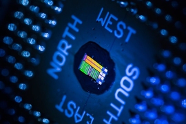
Trapped ions are probably the most widely studied qubit technology, but they’ve historically required a large and complex hardware apparatus. In today’s Nature Nanotechnology, researchers from MIT and MIT Lincoln Laboratory report an important step toward practical quantum computers, with a paper describing a prototype chip that can trap ions in an electric field and, with built-in optics, direct laser light toward each of them.
“If you look at the traditional assembly, it’s a barrel that has a vacuum inside it, and inside that is this cage that’s trapping the ions. Then there’s basically an entire laboratory of external optics that are guiding the laser beams to the assembly of ions,” says Rajeev Ram, an MIT professor of electrical engineering and one of the senior authors on the paper. “Our vision is to take that external laboratory and miniaturize much of it onto a chip.”
Caged in
The Quantum Information and Integrated Nanosystems group at Lincoln Laboratory was one of several research groups already working to develop simpler, smaller ion traps known as surface traps. A standard ion trap looks like a tiny cage, whose bars are electrodes that produce an electric field. Ions line up in the center of the cage, parallel to the bars. A surface trap, by contrast, is a chip with electrodes embedded in its surface. The ions hover 50 micrometers above the electrodes.
Cage traps are intrinsically limited in size, but surface traps could, in principle, be extended indefinitely. With current technology, they would still have to be held in a vacuum chamber, but they would allow many more qubits to be crammed inside.
“We believe that surface traps are a key technology to enable these systems to scale to the very large number of ions that will be required for large-scale quantum computing,” says Jeremy Sage, who together with John Chiaverini leads Lincoln Laboratory’s trapped-ion quantum-information-processing project. “These cage traps work very well, but they really only work for maybe 10 to 20 ions, and they basically max out around there.”
Performing a quantum computation, however, requires precisely controlling the energy state of every qubit independently, and trapped-ion qubits are controlled with laser beams. In a surface trap, the ions are only about 5 micrometers apart. Hitting a single ion with an external laser, without affecting its neighbors, is incredibly difficult; only a few groups had previously attempted it, and their techniques weren’t practical for large-scale systems.
Getting onboard
That’s where Ram’s group comes in. Ram and Karan Mehta, an MIT graduate student in electrical engineering and first author on the new paper, designed and built a suite of on-chip optical components that can channel laser light toward individual ions. Sage, Chiaverini, and their Lincoln Lab colleagues Colin Bruzewicz and Robert McConnell retooled their surface trap to accommodate the integrated optics without compromising its performance. Together, both groups designed and executed the experiments to test the new system.
“Typically, for surface electrode traps, the laser beam is coming from an optical table and entering this system, so there’s always this concern about the beam vibrating or moving,” Ram says. “With photonic integration, you’re not concerned about beam-pointing stability, because it’s all on the same chip that the electrodes are on. So now everything is registered against each other, and it’s stable.”
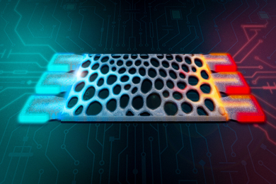
The researchers’ new chip is built on a quartz substrate. On top of the quartz is a network of silicon nitride “waveguides,” which route laser light across the chip. Above the waveguides is a layer of glass, and on top of that are niobium electrodes with tiny holes in them to allow light to pass through. Beneath the holes in the electrodes, the waveguides break into a series of sequential ridges, a “diffraction grating” precisely engineered to direct light up through the holes and concentrate it into a beam narrow enough that it will target a single ion, 50 micrometers above the surface of the chip.
Prospects
With the prototype chip, the researchers were evaluating the performance of the diffraction gratings and the ion traps, but there was no mechanism for varying the amount of light delivered to each ion. In ongoing work, the researchers are investigating the addition of light modulators to the diffraction gratings, so that different qubits can simultaneously receive light of different, time-varying intensities. That would make programming the qubits more efficient, which is vital in a practical quantum information system, since the number of quantum operations the system can perform is limited by the “coherence time” of the qubits.
“As far as I know, this is the first serious attempt to integrate optical waveguides in the same chip as an ion trap, which is a very significant step forward on the path to scaling up ion-trap quantum information processors [QIP] to the sort of size which will ultimately contain the number of qubits necessary for doing useful QIP,” says David Lucas, a professor of physics at Oxford University. “Trapped-ion qubits are well-known for being able to achieve record-breaking coherence times and very precise operations on small numbers of qubits. Arguably, the most important area in which progress needs to be made is technologies which will enable the systems to be scaled up to larger numbers of qubits. This is exactly the need being addressed so impressively by this research.”
“Of course, it's important to appreciate that this is a first demonstration,” Lucas adds. “But there are good prospects for believing that the technology can be improved substantially. As a first step, it's a wonderful piece of work.”


