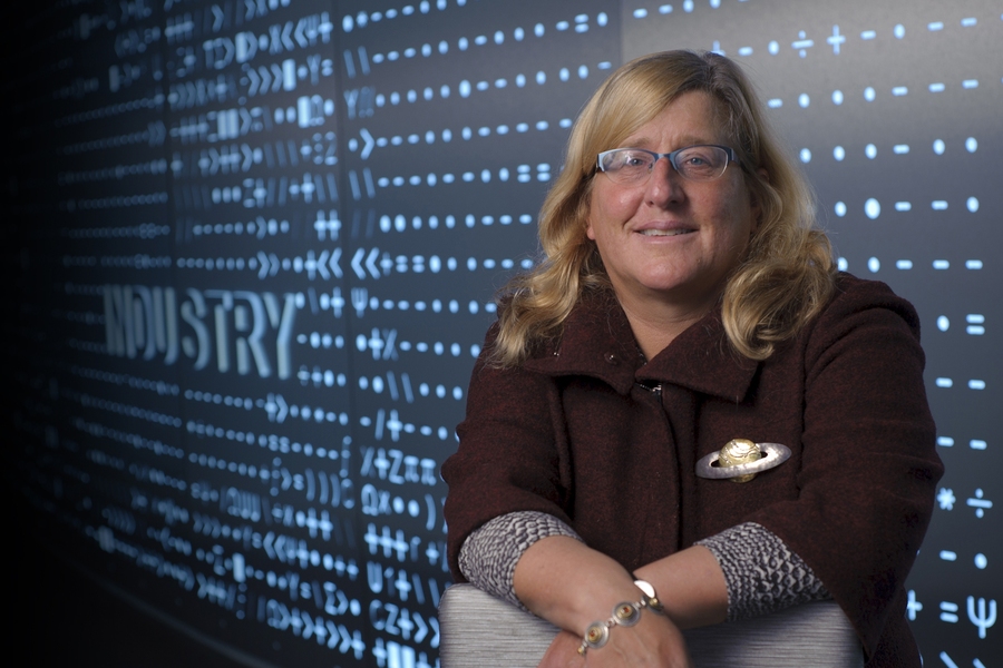
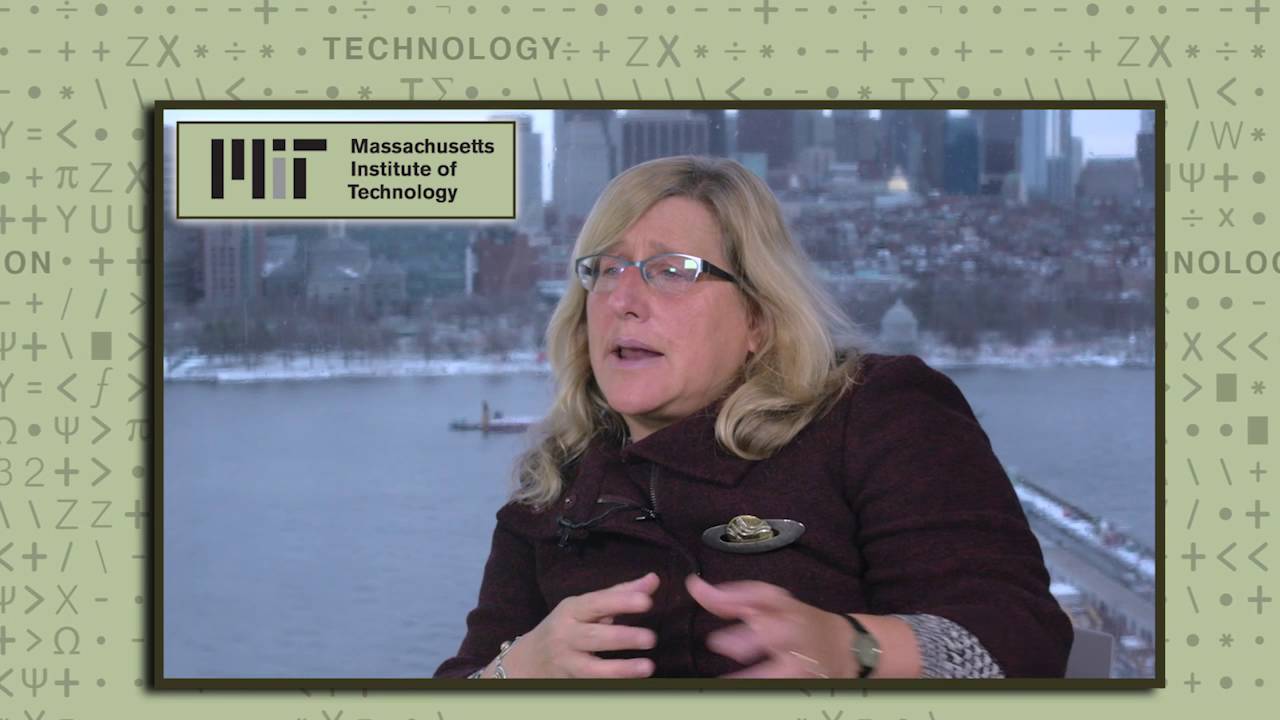
With innovation, there are many truisms, but here are just two. Progress is often made on the nanoscale, and no one company has a monopoly on good ideas in this arena. Karen Gleason has experienced the former and ensures the continuation of the latter. As a professor of chemical engineering, she’s designed an ultrathin coating process that’s benefited rubber manufacturing and holds the potential to speed up computers and help address the global water crisis. As MIT’s associate provost, she manages space issues and industrial relationships, with an intent to encourage even more companies into the already crowded innovation ecosystem surrounding the MIT campus. That density is a key element, she says, in order to continue to produce technology that works not only in a theoretical sense, but also, more importantly, that answers real-world needs and problems.
When membranes last longer
Gleason’s academic focus is on modifying surfaces at the nanoscale and then translating those improvements to larger areas and higher-volume commercial uses. Among other things, she's created a suite of chemical vapor deposition (CVD) processes, which represent, as she says, a platform technology. These microscopic layers have led her to co-found two companies. GVD Corporation started in 2001 and works with rubber manufacturing; applied to molds, GVD’s polymer release coating is durable for months and fully covers the tread features, allowing tires to be easily removed, she says. DropWise, established in 2014, utilizes a related technique on metal surfaces, particularly heat exchangers, improving their heat transfer and thermal performance.
The new CVD process is free of solvent and operates at low temperatures to produce organic materials with a broader range of potential uses. One area with particular potential, Gleason says, is water desalination. In the commonly-used method of reverse osmosis, microbes and molecules accumulate on — and end up fouling — the membranes in this filtration process. Her antibiofouling coating wouldn’t negatively affect the speed at which water would be desalinated, but would allow the membranes to last longer and need less maintenance, thus lowering operating costs, she says.
Reverse osmosis, though, isn’t all-encompassing for water purification. It’s not economical in remote areas where a big plant is not commercially viable. In these cases, Gleason says that her CVD technology can be applied inside microfluidic devices that operate by an electrical current to separate salt ions and are more portable and less expensive since they handle smaller quantities of water. Reverse osmosis is also difficult to use in places where sea water has a high saline percentage, as too large of a pressure across the membrane would be required. Instead, multi-stage flash distillation is an alternative. The process essentially boils water in a series of stages without needing membranes, and treating the inside of the distillation unit would slow the formation of salt and lower the frequency of cleaning, she says.
Regardless of the technique, “the idea is to have the process run more reliably and without intervention,” says Gleason, adding that the result would be more drinkable and usable water in more locations around the world for a lower cost. The technology has been lab-tested on 4-by-6-inch samples. Scaling up isn’t a concern, she says, as she’s done it effectively with CVD reactors before. What is needed is to partner with companies that can test particular surface chemistries for reliability and durability.
Outside of water purification application, Gleason says that CVD polymers could benefit any company making semiconductors. That industry’s desire is to continually shrink dimensions in order to improve performance. With devices like laptops and iPads, companies would like to bring the feature size down below 22 nanometers. As perspective, the typical diameter of human hair is 100 microns, which equates to 100,000 nanometers. Gleason says that CVD polymer technology can hit 7-nanometer feature sizes, adding that her method allows for superior process control and higher purity films, resulting in a higher, more consistent yield of successful devices. The next step is to partner with a vendor in order to vet the technology in an industrial setting and make commercial tools and processes available to chip manufacturers.
Growing the field
As MIT’s associate provost for over two years, Gleason says that a main focus has been to continue a decades-long thrust to enhance the already recognized innovation ecosystem in and around MIT. At its root is an interdisciplinary approach that’s always been a part of the campus. The Institute’s original buildings, she says, were intentionally interconnected by design 100 years ago. People would be near each other and inevitably have chance discussions, blurring the boundaries between departments.
That collaborative attitude has continued, but there’s another component involved, an expectation that innovation doesn’t stop at the boundaries of campus. “It’s not enough to have an original idea,” Gleason says. “You have to make that idea work for the world.” It’s not an approach that’s embraced by every university. There’s a common reluctance that an industrial end use will limit intellectual discovery. She’s found the inverse to be true. “By trying to take your idea out, you ask a different set of questions and come back richer for the experience,” Gleason says.
With GVD, for example, she learned that “markets are harder than molecules.” It was easy to control testing conditions in the lab, but talking to companies about their challenges forces scientists and engineers to address less predictable evaluation parameters in order to produce a product that is responsive to the market.
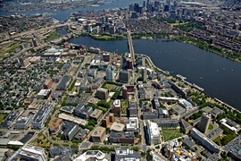
There’s always been a draw to the Kendall Square area that surrounds the eastern side of the MIT campus. Companies have access to faculty, students, postdocs, and former CEOs looking for their next endeavor. Tech, biotech, and biopharma companies are heavily represented. Gleason says that last year the Commonwealth of Massachusetts had more biotech initial public offerings than Silicon Valley. The Cambridge Innovation Center, started in 1999, alone houses over 800 companies, mostly startups. MIT’s Kendall Square Initiative will add six buildings, equaling 1.6 million new square feet for academic and commercial uses, over the next four to 10 years. Additionally, in 2018, a new 200,000 square foot laboratory will open in the center of campus. Known as MIT.nano, it will be able to support 2,000 researchers annually and house shared cleanrooms and state-of-the-art imaging facilities, along with spaces for education, collaboration, and the production of prototypes, all with the intent of advancing the frontiers of technology at the nanoscale.
Gleason says that she would actually like to see more companies adjacent to campus, representing a broader range of industries, including robotics, lighting, and digital health care. This density would facilitate the chance to partner more rapidly and successfully navigate the shared hurdles that all companies, especially new ones, face. “As Lita Nelson, the former head of MIT’s Technology Licensing Office, often quipped, ‘Tech transfer is a contact sport.’ You need other players on the field,” Gleason says. “The richer the environment, the better it is for everybody.”