Microelectromechanical systems — or MEMS — were a $12 billion business in 2014. But that market is dominated by just a handful of devices, such as the accelerometers that reorient the screens of most smartphones.
That’s because manufacturing MEMS has traditionally required sophisticated semiconductor fabrication facilities, which cost tens of millions of dollars to build. Potentially useful MEMS have languished in development because they don’t have markets large enough to justify the initial capital investment in production.
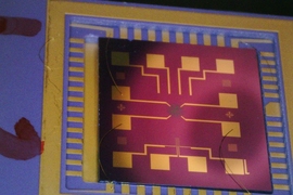
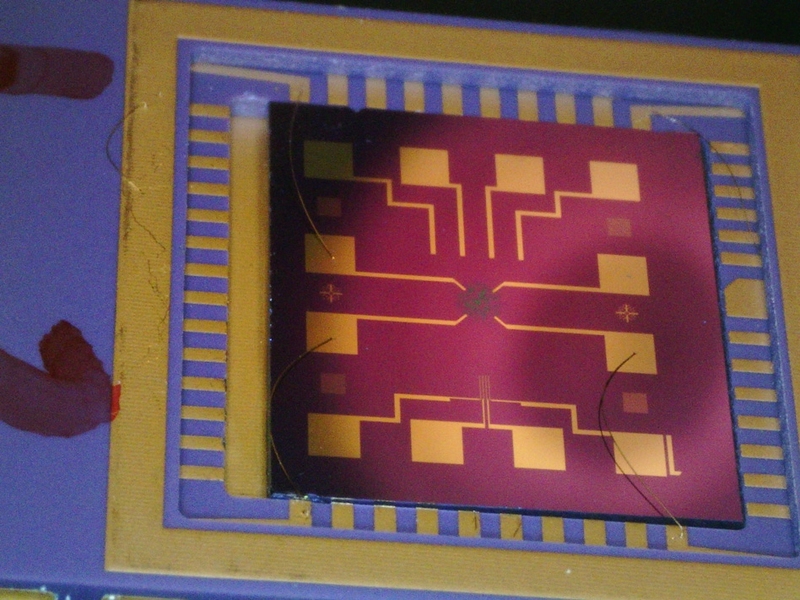
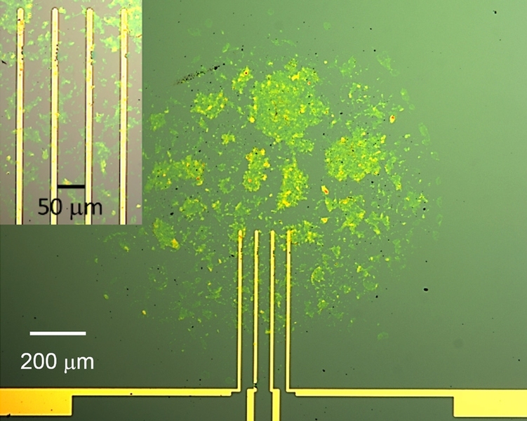
Two recent papers from researchers at MIT’s Microsystems Technologies Laboratories offer hope that that might change. In one, the researchers show that a MEMS-based gas sensor manufactured with a desktop device performs at least as well as commercial sensors built at conventional production facilities.
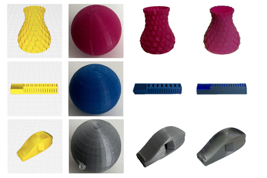
In the other paper, they show that the central component of the desktop fabrication device can itself be built with a 3-D printer. Together, the papers suggest that a widely used type of MEMS gas sensor could be produced at one-hundredth the cost with no loss of quality.
The researchers’ fabrication device sidesteps many of the requirements that make conventional MEMS manufacture expensive. “The additive manufacturing we’re doing is based on low temperature and no vacuum,” says Luis Fernando Velásquez-García, a principal research scientist in MIT’s Microsystems Technology Laboratories and senior author on both papers. “The highest temperature we’ve used is probably 60 degrees Celsius. In a chip, you probably need to grow oxide, which grows at around 1,000 degrees Celsius. And in many cases the reactors require these high vacuums to prevent contamination. We also make the devices very quickly. The devices we reported are made in a matter of hours from beginning to end.”
Welcome resistance
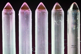
For years, Velásquez-García has been researching manufacturing techniques that involve dense arrays of emitters that eject microscopic streams of fluid when subjected to strong electric fields. For the gas sensors, Velásquez-García and Anthony Taylor, a visiting researcher from the British company Edwards Vacuum, use so-called “internally fed emitters.” These are emitters with cylindrical bores that allow fluid to pass through them.
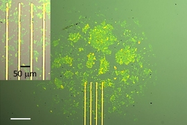
In this case, the fluid contained tiny flakes of graphene oxide. Discovered in 2004, graphene is an atom-thick form of carbon with remarkable electrical properties. Velásquez-García and Taylor used their emitters to spray the fluid in a prescribed pattern on a silicon substrate. The fluid quickly evaporated, leaving a coating of graphene oxide flakes only a few tens of nanometers thick.
The flakes are so thin that interaction with gas molecules changes their resistance in a measurable way, making them useful for sensing. “We ran the gas sensors head to head with a commercial product that cost hundreds of dollars,” Velásquez-García says. “What we showed is that they are as precise, and they are faster. We make at a very low cost — probably cents — something that works as well as or better than the commercial counterparts.”
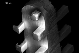
To produce those sensors, Velásquez-García and Taylor used electrospray emitters that had been built using conventional processes. However, in the December issue of the Journal of Microelectromechanical Systems, Velásquez-García reports using an affordable, high-quality 3-D printer to produce plastic electrospray emitters whose size and performance match those of the emitters that yielded the gas sensors.
Made to order
In addition to making electrospray devices more cost-effective, Velásquez-García says, 3-D printing also makes it easier to customize them for particular applications. “When we started designing them, we didn’t know anything,” Velásquez-García says. “But at the end of the week, we had maybe 15 generations of devices, where each design worked better than the previous versions.”
Indeed, Velásquez-García says, the advantages of electrospray are not so much in enabling existing MEMS devices to be made more cheaply as in enabling wholly new devices. Besides making small-market MEMS products cost-effective, electrospray could enable products incompatible with existing manufacturing techniques.
“In some cases, MEMS manufacturers have to compromise between what they intended to make, based on the models, and what you can make based on the microfabrication techniques,” Velásquez-García says. “Only a few devices that fit into the description of having large markets and not having subpar performance are the ones that have made it.”
Electrospray could also lead to novel biological sensors, Velásquez-García says. “It allows us to deposit materials that would not be compatible with high-temperature semiconductor manufacturing, like biological molecules,” he says.
“For sure, the paper opens new technical paths to making gas microsensors,” says Jan Dziuban, head of the Division of Microengineering at Wroclaw University of Technology in Poland. “From a technical point of view, the process may be easily adapted to mass fabrication.”
“But promising results must be proved statistically,” he cautions. “Personal experience tells me that plenty of very promising materials for new sensors, utilizing nanostructured materials, which have been published in high-level scientific papers, haven't resulted in reliable products.”
