Nanofibers — strands of material only a couple hundred nanometers in diameter — have a huge range of possible applications: scaffolds for bioengineered organs, ultrafine air and water filters, and lightweight Kevlar body armor, to name just a few. But so far, the expense of producing them has consigned them to a few high-end, niche applications.
Luis Velásquez-García, a principal research scientist at MIT’s Microsystems Technology Laboratories, and his group hope to change that. At the International Workshop on Micro and Nanotechnology for Power Generation and Energy Conversion Applications in December, Velásquez-García, his student Philip Ponce de Leon, and Frances Hill, a postdoc in his group, will describe a new system for spinning nanofibers that should offer significant productivity increases while drastically reducing power consumption.
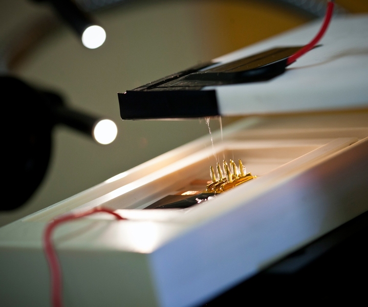
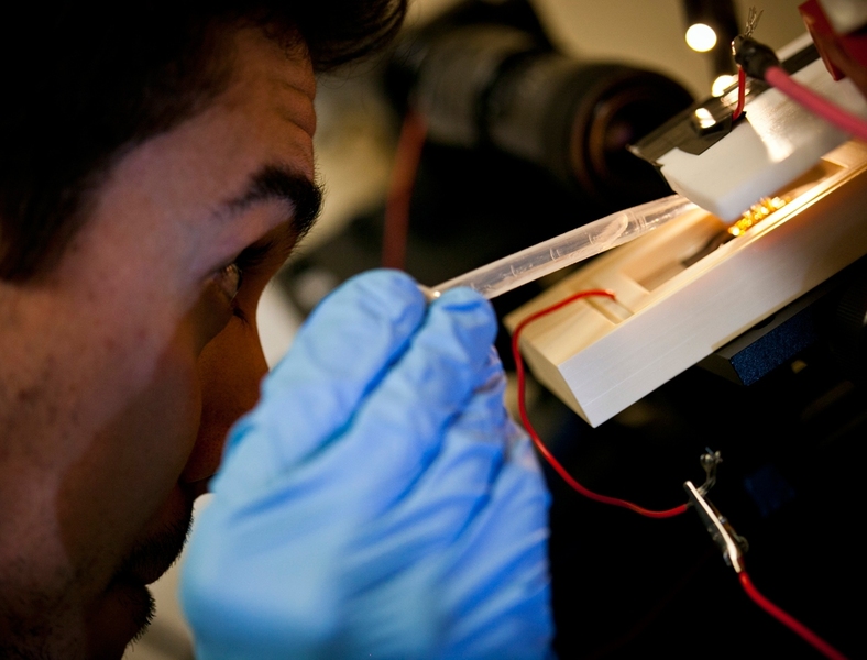
Using manufacturing techniques common in the microchip industry, the MTL researchers built a one-square-centimeter array of conical tips, which they immersed in a fluid containing a dissolved plastic. They then applied a voltage to the array, producing an electrostatic field that is strongest at the tips of the cones. In a technique known as electrospinning, the cones eject the dissolved plastic as a stream that solidifies into a fiber only 220 nanometers across.
In their experiments, the researchers used a five-by-five array of cones, which already yields a sevenfold increase in productivity per square centimeter over even the best existing methods. But, Velásquez-García says, it should be relatively simple to pack more cones onto a chip, boosting productivity even more. Indeed, he says, in prior work on a similar technique called electrospray, his lab was able to cram almost a thousand emitters into a single square centimeter. And multiple arrays could be combined in a panel to further increase yields.
Surfaces, from scratch
Because the new paper was prepared for an energy conference, it focuses on energy applications. But nanofibers could be useful for any device that needs to maximize the ratio of surface area to volume, Velásquez-García says. Capacitors — circuit components that store electricity — are one example, because capacitance scales with surface area. The electrodes used in fuel cells are another, because the greater the electrodes’ surface area, the more efficiently they catalyze the reactions that drive the cell. But almost any chemical process can benefit from increasing catalysts’ surface area, and increasing the surface area of artificial-organ scaffolds gives cells more points at which to adhere.
Another promising application of nanofibers is in meshes so fine that they allow only nanoscale particles to pass through. The example in the new paper again comes from energy research: the membranes that separate the halves of a fuel cell. But similar meshes could be used to filter water. Such applications, Velásquez-García says, depend crucially on consistency in the fiber diameter, another respect in which the new technique offers advantages over its predecessors.
Existing electrospinning techniques generally rely on tiny nozzles, through which the dissolved polymer is forced. Variations in operating conditions and in the shape of the nozzles can cause large variation in the fiber diameter, and the nozzles’ hydraulics mean that they can’t be packed as tightly together. A few manufacturers have developed fiber-spinning devices that use electrostatic fields, but their emitters are made using much cruder processes than the chip-manufacturing techniques that the MTL researchers exploited. As a consequence, not only are the arrays of tips much less dense, but the devices consume more power.
“The electrostatic field is enhanced if the tip diameter is smaller,” Velásquez-García says. “If you have tips of, say, millimeter diameter, then if you apply enough voltage, you can trigger the ionization of the liquid and spin fibers. But if you can make them sharper, then you need a lot less voltage to achieve the same result.”
Wicked wicker
The use of microfabrication technologies not only allowed the MTL researchers to pack their cones more tightly and sharpen their tips, but it also gave them much more precise control of the structure of the cones’ surfaces. Indeed, the sides of the cones have a nubby texture that helps the cones wick up the fluid in which the polymer is dissolved. In ongoing experiments, the researchers have also covered the cones with what Velásquez-García describes as a “wool” of carbon nanotubes, which should work better with some types of materials.
Indeed, Velásquez-García says, his group’s results depend not only on the design of the emitters themselves, but on a precise balance between the structure of the cones and their textured coating, the strength of the electrostatic field, and the composition of the fluid bath in which the cones are immersed.
“Fabricating exactly identical emitters in parallel with high precision and a lot of throughput — this is their main contribution, in my opinion,” says Antonio Luque Estepa, an associate professor of electrical engineering at the University of Seville who specializes in electrospray deposition and electrospinning. “Fabricating one is easy. But 100 or 1,000 of them, that’s not so easy. Many times there are problems with interactions between one output and the output next to it.”
The microfabrication technique that Velásquez-García’s group employs, Luque adds, “does not limit the number of outputs that they can integrate on one chip.” Although the extent to which the group can increase emitter density remains to be seen, Luque says, he’s confident that “they can make a tenfold increase over what is available right now.”
The MIT researchers’ work was funded in part by the U.S. Defense Advanced Research Projects Agency.