As the United States seeks to reinvigorate its job market and move past economic recession, MIT News examines manufacturing’s role in the country’s economic future through this series on work at the Institute around manufacturing.
In the last decade, MEMS (microelectromechanical devices) have wrought revolutions in several industries: Arrays of micromirrors, for instance, enabled digital film projectors, and accelerometers like those in Nintendo’s Wii controller have changed gaming. But commercially successful MEMS represent a tiny sampling of the prototypes developed in academic and industry labs — from supersensitive biological sensors to films that can turn any surface into a loudspeaker to devices that harvest energy from motion.
The problem is that most current MEMS are built using the same techniques used to produce computer chips, and those techniques are expensive. “Over the past 20 or 30 years, the cost of a tool that performs a specific function in a semiconductor manufacturing plant has risen quite dramatically — orders of magnitude,” says Martin Schmidt, a professor of electrical engineering and associate provost at MIT. “As these capital costs have escalated, the minimum market you need to be able to access just keeps going up.” Many experimental MEMS — as ingenious and even useful as they may be — simply don’t command markets large enough to justify the expense of building a new manufacturing facility.
By the same token, however, semiconductor manufacturing has such high capital costs that exporting it may not be cost-effective. “It’s not about labor costs, because the capital costs are paramount,” Schmidt says. As a consequence, “if a particular government or region of the world is willing to subsidize the access to capital to create those facilities, you can cause the growth of that industry in your area.”
Schmidt points to Abu Dhabi, which is emerging as a center of semiconductor manufacture, even though per-capita income in the United Arab Emirates is higher than it is in the United States, and to the Albany NanoTech complex in Albany, N.Y., which is funded by industry in exchange for state investments in local educational institutions and in energy efficiency. Indeed, Schmidt says, the investment that the Defense Advanced Research Projects Agency (DARPA) made in MEMS in the 1990s bears a great deal of credit for the relatively small number of MEMS success stories.
Alternate routes
But federal investment in MEMS isn’t what it once was, and Schmidt isn’t just waiting around for it to return. “The question is, ‘Are there technology disruptions that can drive [MEMS manufacture]?’” he says. “If you imagine you’ve conceived of ways to manufacture at the micro- and nanoscale, but you’ve conceived of them in a way that the capital was scalable, then maybe the capital cost is less intimidating. So I may not be driven to put my plant somewhere else in the world, because the capital cost is well-matched to the size of my market.”
Moreover, Schmidt says — echoing the argument made by electrical engineering and computer science professor Judy Hoyt in a previous installment in the Future of Manufacturing series — “there’s a number of folks who feel quite strongly that in order to innovate in products, one has to understand the processes by which these products are made. And one of the best ways to understand the processes by which these products are made is to have the manufacturing in physical proximity.”
Schmidt’s own research focuses on building MEMS by using ink-jet printing technology to deposit metallic nanoparticles on some type of substrate. “We’ve made some very rudimentary MEMS structures,” Schmidt says, “and they have functionally the same behavior as MEMS formed using conventional techniques.” He also points to the research of Vladimir Bulović, whose laboratory is investigating low-cost methods of manufacturing MEMS by stamping patterns into plastics.
MEMS unmasked
Henry Smith, a professor of electrical engineering, is developing a scalable manufacturing technique that bears greater resemblance to the standard method for producing chips. Traditionally, chips are built up in layers, through a process known as photolithography. Each layer consists of a different material, and a functional pattern is transferred to it by light passing through a stencil, or “mask.”
In fact, the masks themselves are one of the major expenses in chip manufacturing; Smith’s technique does away with them. Instead, it produces patterns using an array of 1,000 tiny lenses. A wafer of material moves back and forth beneath the lenses, and the light passing through them turns on and off. Where photolithography can, at best, transfer a pattern to a rectangle that’s 20 millimeters by 30 millimeters, Smith’s technique can impart a single pattern to the entire surface of a six-inch wafer.
“Moreover,” Smith says, “as impressive as integrated circuits are, the only thing on them is transistors, transistors and wires. Now, a MEMS device might have a diving board, a heavy weight here, a rotating part there — every single MEMS device is different than the previous one.” With its 1,000 beams of light flashing on and off as they scan across the wafer, Smith’s system can impart one set of arbitrary patterns to one wafer and a completely different pattern to the next.
Smith founded a company, called LumArray, to commercialize his system. The firm has already sold one machine to the National Institute of Standards and Technology and is delivering another to the Defense Microelectronic Activity.
One for all
Of course, market size wouldn’t be a problem for MEMS manufacturers if they could simply share fabrication facilities, collectively shouldering the expense of construction. But MEMS tend to have their own idiosyncratic manufacturing requirements, and no existing facilities can handle more than a few closely related devices.
Research at MIT could help address that problem, too. It could also aid with retrofitting older facilities that are no longer adequate for the manufacture of state-of-the-art chips, but which have recouped their capital costs — a strategy that some domestic MEMS manufacturers already employ.
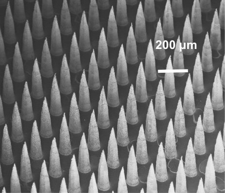
In work funded not only by DARPA but also by NASA and the U.S. Navy, Luis Fernando Velásquez-García, a principal research scientist at MIT’s Microsystems Technology Laboratory, designs MEMS, many of which exploit dense arrays of tiny cylinders with conical tips. That shared fundamental design yields a remarkable number of applications: vacuum amplifiers for radio-frequency systems, biological and chemical sensors with low false-positive rates, a fiber-spinning system for producing flexible materials with remarkable properties, propulsion systems for tiny satellites, and portable X-ray sources.
Yet another application of that basic design, however, is a family of tiny plasma sensors. Today, plasmas — gases with ionized, or electrically charged, atoms — are used in MEMS and microchip manufacture to both deposit materials and to etch patterns into them. But precisely controlling the plasmas is one of the manufacturing problems that has to be solved over and over again for each new device. “If you were able to make these sensors at low cost, so that you could put them in every plasma reactor, you could have better control of your process,” Velásquez-García says.
Measure twice
Jacob White, the Cecil H. Green Professor of Electrical Engineering and Computer Science, develops computer-aided design (CAD) tools for engineering applications. These days, his academic research focuses more on biological and biomedical devices, but in the past, he’s worked on CAD systems for MEMS as well. Modern CAD systems — White’s included — don’t just provide intuitive visual interfaces for device design; they also include simulation software that verifies the devices’ performance, a process known as computational prototyping.
Today, White says, “when engineers design a digital integrated circuit, the chances are very high that their very first attempt at fabrication will work, because the simulation tools are so complete.” That’s not true in the MEMS industry, White says, where the CAD tools “are nowhere near as comprehensive.”
In principle, better CAD tools could lead to MEMS with higher production yields and designs that are better tailored to the processes available at particular manufacturing facilities. But, White explains, MEMS CAD is another casualty of the general decline in MEMS funding. “We got so far but no further,” he says. But in the last 10 years or so, he says, research on CAD tools for other applications has made great strides. “If [MEMS CAD] became a real push, there are a lot of numerical advances that could be put into the problem,” he says.
Nor is it far-fetched that a “real push” on MEMS CAD could pay dividends for U.S. manufacturing. “DARPA invested heavily in integrated-circuit CAD in the ’80s,” White says. “Many people think that revitalized the U.S. semiconductor industry.”
In the last decade, MEMS (microelectromechanical devices) have wrought revolutions in several industries: Arrays of micromirrors, for instance, enabled digital film projectors, and accelerometers like those in Nintendo’s Wii controller have changed gaming. But commercially successful MEMS represent a tiny sampling of the prototypes developed in academic and industry labs — from supersensitive biological sensors to films that can turn any surface into a loudspeaker to devices that harvest energy from motion.
The problem is that most current MEMS are built using the same techniques used to produce computer chips, and those techniques are expensive. “Over the past 20 or 30 years, the cost of a tool that performs a specific function in a semiconductor manufacturing plant has risen quite dramatically — orders of magnitude,” says Martin Schmidt, a professor of electrical engineering and associate provost at MIT. “As these capital costs have escalated, the minimum market you need to be able to access just keeps going up.” Many experimental MEMS — as ingenious and even useful as they may be — simply don’t command markets large enough to justify the expense of building a new manufacturing facility.
By the same token, however, semiconductor manufacturing has such high capital costs that exporting it may not be cost-effective. “It’s not about labor costs, because the capital costs are paramount,” Schmidt says. As a consequence, “if a particular government or region of the world is willing to subsidize the access to capital to create those facilities, you can cause the growth of that industry in your area.”
Schmidt points to Abu Dhabi, which is emerging as a center of semiconductor manufacture, even though per-capita income in the United Arab Emirates is higher than it is in the United States, and to the Albany NanoTech complex in Albany, N.Y., which is funded by industry in exchange for state investments in local educational institutions and in energy efficiency. Indeed, Schmidt says, the investment that the Defense Advanced Research Projects Agency (DARPA) made in MEMS in the 1990s bears a great deal of credit for the relatively small number of MEMS success stories.
Alternate routes
But federal investment in MEMS isn’t what it once was, and Schmidt isn’t just waiting around for it to return. “The question is, ‘Are there technology disruptions that can drive [MEMS manufacture]?’” he says. “If you imagine you’ve conceived of ways to manufacture at the micro- and nanoscale, but you’ve conceived of them in a way that the capital was scalable, then maybe the capital cost is less intimidating. So I may not be driven to put my plant somewhere else in the world, because the capital cost is well-matched to the size of my market.”
Moreover, Schmidt says — echoing the argument made by electrical engineering and computer science professor Judy Hoyt in a previous installment in the Future of Manufacturing series — “there’s a number of folks who feel quite strongly that in order to innovate in products, one has to understand the processes by which these products are made. And one of the best ways to understand the processes by which these products are made is to have the manufacturing in physical proximity.”
Schmidt’s own research focuses on building MEMS by using ink-jet printing technology to deposit metallic nanoparticles on some type of substrate. “We’ve made some very rudimentary MEMS structures,” Schmidt says, “and they have functionally the same behavior as MEMS formed using conventional techniques.” He also points to the research of Vladimir Bulović, whose laboratory is investigating low-cost methods of manufacturing MEMS by stamping patterns into plastics.
MEMS unmasked
Henry Smith, a professor of electrical engineering, is developing a scalable manufacturing technique that bears greater resemblance to the standard method for producing chips. Traditionally, chips are built up in layers, through a process known as photolithography. Each layer consists of a different material, and a functional pattern is transferred to it by light passing through a stencil, or “mask.”
In fact, the masks themselves are one of the major expenses in chip manufacturing; Smith’s technique does away with them. Instead, it produces patterns using an array of 1,000 tiny lenses. A wafer of material moves back and forth beneath the lenses, and the light passing through them turns on and off. Where photolithography can, at best, transfer a pattern to a rectangle that’s 20 millimeters by 30 millimeters, Smith’s technique can impart a single pattern to the entire surface of a six-inch wafer.
“Moreover,” Smith says, “as impressive as integrated circuits are, the only thing on them is transistors, transistors and wires. Now, a MEMS device might have a diving board, a heavy weight here, a rotating part there — every single MEMS device is different than the previous one.” With its 1,000 beams of light flashing on and off as they scan across the wafer, Smith’s system can impart one set of arbitrary patterns to one wafer and a completely different pattern to the next.
Smith founded a company, called LumArray, to commercialize his system. The firm has already sold one machine to the National Institute of Standards and Technology and is delivering another to the Defense Microelectronic Activity.
One for all
Of course, market size wouldn’t be a problem for MEMS manufacturers if they could simply share fabrication facilities, collectively shouldering the expense of construction. But MEMS tend to have their own idiosyncratic manufacturing requirements, and no existing facilities can handle more than a few closely related devices.
Research at MIT could help address that problem, too. It could also aid with retrofitting older facilities that are no longer adequate for the manufacture of state-of-the-art chips, but which have recouped their capital costs — a strategy that some domestic MEMS manufacturers already employ.
In work funded not only by DARPA but also by NASA and the U.S. Navy, Luis Fernando Velásquez-García, a principal research scientist at MIT’s Microsystems Technology Laboratory, designs MEMS, many of which exploit dense arrays of tiny cylinders with conical tips. That shared fundamental design yields a remarkable number of applications: vacuum amplifiers for radio-frequency systems, biological and chemical sensors with low false-positive rates, a fiber-spinning system for producing flexible materials with remarkable properties, propulsion systems for tiny satellites, and portable X-ray sources.
Yet another application of that basic design, however, is a family of tiny plasma sensors. Today, plasmas — gases with ionized, or electrically charged, atoms — are used in MEMS and microchip manufacture to both deposit materials and to etch patterns into them. But precisely controlling the plasmas is one of the manufacturing problems that has to be solved over and over again for each new device. “If you were able to make these sensors at low cost, so that you could put them in every plasma reactor, you could have better control of your process,” Velásquez-García says.
Measure twice
Jacob White, the Cecil H. Green Professor of Electrical Engineering and Computer Science, develops computer-aided design (CAD) tools for engineering applications. These days, his academic research focuses more on biological and biomedical devices, but in the past, he’s worked on CAD systems for MEMS as well. Modern CAD systems — White’s included — don’t just provide intuitive visual interfaces for device design; they also include simulation software that verifies the devices’ performance, a process known as computational prototyping.
Today, White says, “when engineers design a digital integrated circuit, the chances are very high that their very first attempt at fabrication will work, because the simulation tools are so complete.” That’s not true in the MEMS industry, White says, where the CAD tools “are nowhere near as comprehensive.”
In principle, better CAD tools could lead to MEMS with higher production yields and designs that are better tailored to the processes available at particular manufacturing facilities. But, White explains, MEMS CAD is another casualty of the general decline in MEMS funding. “We got so far but no further,” he says. But in the last 10 years or so, he says, research on CAD tools for other applications has made great strides. “If [MEMS CAD] became a real push, there are a lot of numerical advances that could be put into the problem,” he says.
Nor is it far-fetched that a “real push” on MEMS CAD could pay dividends for U.S. manufacturing. “DARPA invested heavily in integrated-circuit CAD in the ’80s,” White says. “Many people think that revitalized the U.S. semiconductor industry.”