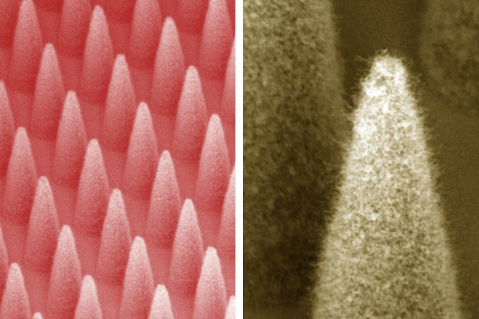


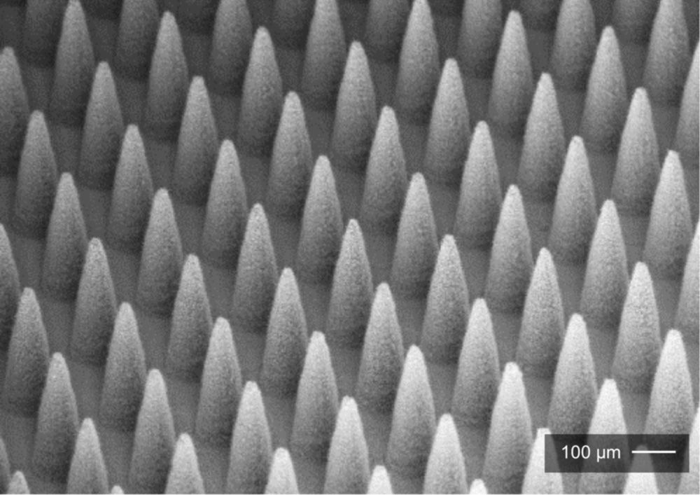

Luis Fernando Velásquez-García’s group at MIT’s Microsystems Technology Laboratories (MTL) develops dense arrays of microscopic cones that harness electrostatic forces to eject streams of ions.
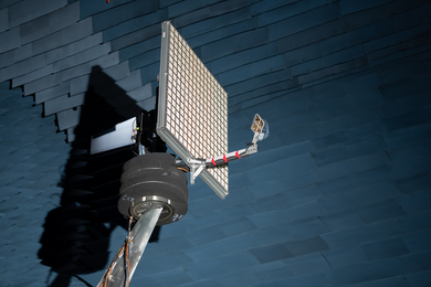
The technology has a range of promising applications: depositing or etching features onto nanoscale mechanical devices; spinning out nanofibers for use in water filters, body armor, and “smart” textiles; or propulsion systems for fist-sized “nanosatellites.”
In the latest issue of the IEEE Journal of Microelectromechanical Systems, Velásquez-García, his graduate students Eric Heubel and Philip Ponce de Leon, and Frances Hill, a postdoc in his group, describe a new prototype array that generates 10 times the ion current per emitter that previous arrays did.
Ion current is a measure of the charge carried by moving ions, which translates directly to the rate at which particles can be ejected. Higher currents thus promise more-efficient manufacturing and more-nimble satellites.
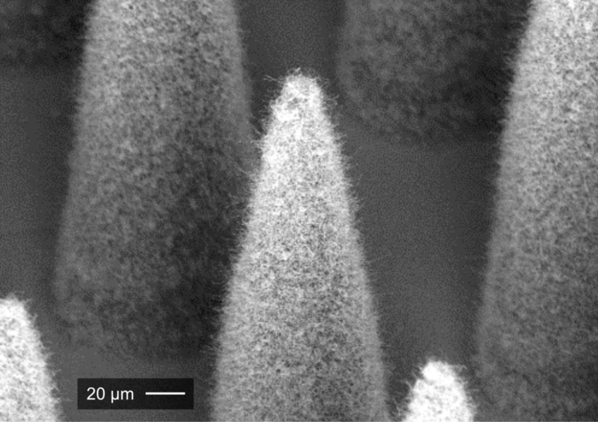
The same prototype also crams 1,900 emitters onto a chip that’s only a centimeter square, quadrupling the array size and emitter density of even the best of its predecessors.
“This is a field that benefits from miniaturizing the components, because scaling down emitters implies less power consumption, less bias voltage to operate them, and higher throughput,” says Velásquez-García, a principal research scientist at MTL. “The topic we have been tackling is how we can make these devices operate as close as we can to the theoretical limit and how we can greatly increase the throughput by virtue of multiplexing, with massively parallel devices that operate uniformly.”
When Velásquez-García speaks of a “theoretical limit,” he’s talking about the point at which droplets — clumps of molecules — rather than ions — individual molecules — begin streaming off of the emitters. Among other problems, droplets are heavier, so their ejection velocity is lower, which makes them less useful for etching or satellite propulsion.
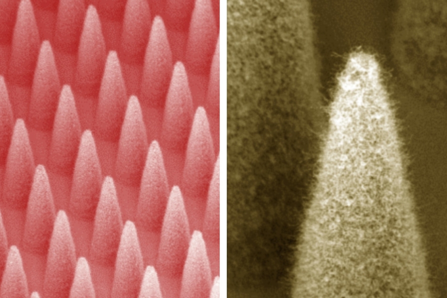
The ions ejected by Velásquez-García’s prototype are produced from an ionic salt that’s liquid at room temperature. Surface tension wicks the fluid up the side of the emitters to the tip of the cone, whose narrowness concentrates the electrostatic field. At the tip, the liquid is ionized and, ideally, ejected one molecule at a time.
Slow the flow
When the ion current in an emitter gets high enough, droplet formation is inevitable. But earlier emitter arrays — those built both by Velásquez-García’s group and by others — fell well short of that threshold.
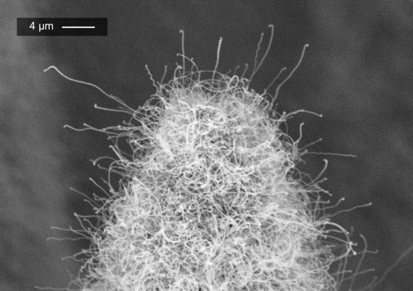
Increasing an array’s ion current is a matter of regulating the flow of the ionic salt up the emitters’ sides. To do that, the MIT researchers had previously used black silicon, a form of silicon grown as closely packed bristles. But in the new work, they instead used carbon nanotubes — atom-thick sheets of carbon rolled into cylinders — grown on the slopes of the emitters like trees on a mountainside.
By carefully tailoring the density and height of the nanotubes, the researchers were able to achieve a fluid flow that enabled an operating ion current at very near the theoretical limit.
“We also show that they work uniformly — that each emitter is doing exactly the same thing,” Velásquez-García says. That’s crucial for nanofabrication applications, in which the depth of an etch, or the height of deposits, must be consistent across an entire chip.
To control the nanotubes’ growth, the researchers first cover the emitter array with an ultrathin catalyst film, which is broken into particles by chemical reactions with both the substrate and the environment. Then they expose the array to a plasma rich in carbon. The nanotubes grow up under the catalyst particles, which sit atop them, until the catalyst degrades.
Increasing the emitter density — the other improvement reported in the new paper — was a matter of optimizing existing manufacturing “recipe,” Velásquez-García says. The emitters, like most nanoscale silicon devices, were produced through photolithography, a process in which patterns are optically transferred to layers of materials deposited on silicon wafers; a plasma then etches the material away according to the pattern. “The recipe is the gases, power, pressure level, time, and the sequence of the etching,” Velásquez-García says. “We started doing electrospray arrays 15 years ago, and making different generations of devices gave us the know-how to make them better.”
Nanoprinting
Velásquez-García believes that using arrays of emitters to produce nanodevices could have several advantages over photolithography — the technique that produces the arrays themselves. Because they can operate at room temperature and don’t require a vacuum chamber, the arrays could deposit materials that can’t withstand the extreme conditions of many micro- and nanomanufacturing processes. And they could eliminate the time-consuming process of depositing new layers of material, exposing them to optical patterns, etching them, and then starting all over again.
“In my opinion, the best nanosystems are going to be done by 3-D printing because it would bypass the problems of standard microfabrication,” Velásquez-García says. “It uses prohibitively expensive equipment, which requires a high level of training to operate, and everything is defined in planes. In many applications you want the three-dimensionality: 3-D printing is going to make a big difference in the kinds of systems we can put together and the optimization that we can do.”
“Typically the interest of this type of emitter is to be able to emit a beam of ions and not a beam of droplets,” says Herbert Shea, an associate professor in the Microsystems for Space Technologies Laboratory at the École Polytechnique Fédérale de Lausanne. “Using their nanotube forest, they’re able to get the devices to operate in pure ion mode but have a high current typically associated with the droplet mode.”
Shea believes that, at least in the near term, the technology’s most promising application is in spacecraft propulsion. “It would take a lot of effort to make it into a practical micromachining tool, whereas it would take very little effort to use it as propulsion for small spacecraft,” he says. “The reason you’d like to be in ion mode is to have the most efficient conversion of the mass of the propellant into the momentum of the spacecraft.”