In 2006, when Tomás Palacios completed his PhD in electrical and computer engineering at the University of California at Santa Barbara, he was torn between taking a job in academia or industry.
“I wanted to make sure that the new ideas that we were generating could find a path toward society,” says Palacios, the newly tenured Emmanuel E. Landsman Associate Professor of Electrical Engineering and Computer Science at MIT. “In industry, I was sure that would happen; I was not sure how it would work in academia.”
“What I found when I came here,” he says, “is that MIT is really an amazing place to get all these new ideas out and to collaborate with industry to make sure that the new concepts and new ideas coming out of the university environment find their place in real products and applications.”
According to Palacios, his research group focuses on the application of what he likes to call “extreme materials” to electronics. The 25 graduate students, postdocs and research scientists in the group are split between two major research projects: One focuses on applications of an exotic material called gallium nitride; the other on applications of graphene — a form of carbon — and other “two-dimensional materials” that consist of crystals just a few atoms thick.
“A very important difference between the effort going on in our group and the work going on other places is that we try very hard to find applications for these materials,” Palacios says. “Of course we are interested in the basic science, but we think that MIT is a place that should contribute very heavily to link basic science to applications.”
High potential
Palacios was born in the Andalucia region of Spain to scientifically minded parents: His father taught high school math, and his mother was a pediatrician. His parents relocated several times when he was young: He spent stretches of several years in the Canary Islands — closer to Morocco than to the Spanish mainland — and in the historic northern Spanish city of León, which was founded in the last years of the Roman Republic. The family finally settled in Madrid, where Palacios went to both high school and the Polytechnic University of Madrid, where he graduated with a five-year degree that he describes as a combination of a bachelor’s and master’s.
Already at the Polytechnic, Palacios had started researching gallium nitride, which was also the subject of his PhD research. But when he arrived at MIT in 2006, “at more or less the same time, there was another revolutionary material being isolated for the first time, and that was graphene,” Palacios says. “So it was very natural for us to get excited about that material.”
Gallium nitride is “extreme,” Palacios says, because it can handle 10 times as much voltage as silicon, which is the basis of most modern electronics. “Graphene is extreme because of many other things: It’s the thinnest material you can think of, it’s the lightest material, it’s the strongest material, it’s the material where the electrons travel most easily,” he says.
With each material, Palacios’ group has identified three main research areas. Because gallium nitride can handle such high voltages, it’s a promising candidate for new types of power electronics — devices like those that convert the 110 volts of the electricity distributed through the power grid to higher or lower voltages.
Indeed, in May, the U.S. Department of Energy (DOE) announced a new, $140 million research institute to focus on power electronics, with roughly half of that money going toward gallium nitride research. In its announcement, the DOE cited a study showing that the adoption of gallium nitride in both lighting and power electronics could reduce worldwide energy consumption by 25 percent.
Because of its high voltage tolerances, gallium nitride could also lead to higher-frequency electronics. “Today, you have cellphones operating at a few gigahertz; some wireless communication systems are working at 20, 30, 40 gigahertz,” Palacios says. “We believe that gallium nitride is going to push the performance of electronics to hundreds of gigahertz or even terahertz.” Using the resources of MIT’s Microsystems Technology Laboratory, Palacios’ group has built some of what he says are among “the fastest gallium nitride transistors in the world.”
For all its performance advantages over silicon, however, gallium nitride is not nearly so abundant — or cheap. So a third area of research in Palacios’ group is techniques for integrating gallium nitride circuits into silicon chips, so that the silicon can handle the run-of-the-mill signal switching.
Faster, stronger
Carbon, on the other hand, is plentiful, so cost effectiveness is, in principle, one of graphene’s attractions. Palacios and his team are investigating the use of graphene in large-area transparent electronics that could be layered onto walls, windows or clothes.
They’re also examining the use of graphene in chemical or biological sensors. Because a layer of graphene is so thin, it’s sensitive to the proximity of even a single molecule — of, say, glucose in a blood sample. And because it’s so electrically conductive, the proximity of a target molecule would register as a very clear change in an electrical signal.
Finally, the group is investigating the use of graphene in a new generation of night-vision systems, which could be mounted in cars to provide warning systems for nighttime driving, among other applications.
“We are able to work on all of these projects thanks to the very collaborative environment that we have found here at MIT,” Palacios says. “I think that that is very, very special about MIT.”
Tomás Palacios investigates use of ‘extreme materials’ in electronics, which could reduce energy consumption and make computers far faster.
Publication Date:

Caption:
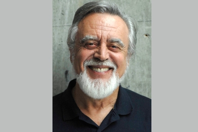
Tomás Palacios
Credits:
Photo: Bryce Vickmark
Caption:
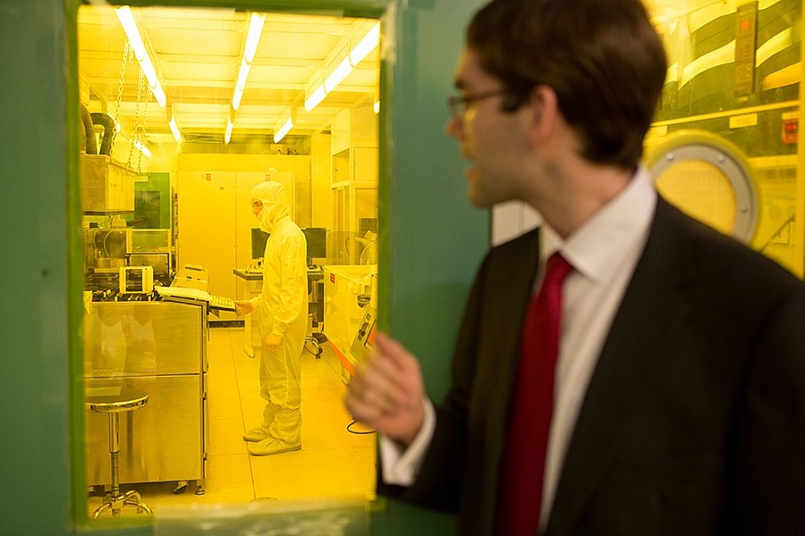
Tomás Palacios peers into the Microsystems Technology Laboratory (MTL) clean room where his record-setting gallium nitride transistors were manufactured.
Credits:
Photo: Bryce Vickmark
Caption:
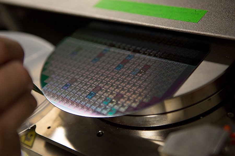
A wafer with hundreds of gallium nitride chips etched into its surface emerges from the MTL production line.
Credits:
Photo: Bryce Vickmark
Press Mentions
The New Yorker
In an article examining graphene, John Colapinto of The New Yorker highlights Prof. Tomas Palacios’ work integrating graphene into everyday objects. “Rather than using graphene to improve existing applications, as Tour’s lab mostly does, Palacios is trying to build devices for a future world,” writes Colapinto.