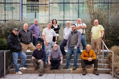
Meet the tight-knit technical staff who help MIT.nano handle any challenge
All together, a core group of MIT.nano staffers has more than 400 years of technical experience in nanoscale characterization and fabrication.
All together, a core group of MIT.nano staffers has more than 400 years of technical experience in nanoscale characterization and fabrication.
Over the course of four days, Indigenous delegates collaborated on immersive technology with MIT community members.
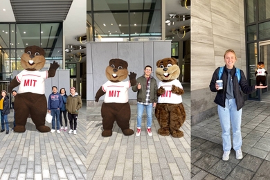
MIT student creates Tim the Beaver in virtual reality using the MIT.nano Immersion Lab.
The Fulbright US Student Program funds opportunities for research, graduate study, and teaching abroad.
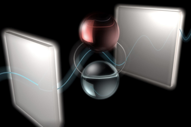
A perovskite-based device that combines aspects of electronics and photonics may open doors to new kinds of computer chips or quantum qubits.
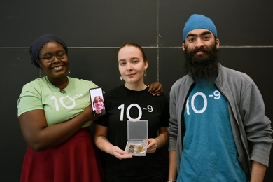
The HUMANS nanowafer, an MIT Space Exploration Initiative student-led project, will travel to the ISS this month, and later to the moon, carrying messages in more than 64 languages from over 80 countries.

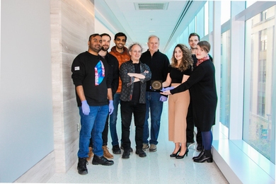
A campus summit with the leader and his delegation centered around dialogue on biotechnology and innovation ecosystems.
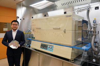
A new low-temperature growth and fabrication technology allows the integration of 2D materials directly onto a silicon circuit, which could lead to denser and more powerful chips.

U.S. Department of Energy selects MIT to establish collaborative research center for optimizing the development of tandem solar modules.
A hands-on class teaches undergraduates the fundamentals of quantum mechanics and nanoscale science from inside MIT.nano’s cleanroom.
In MIT visit, CEO Pat Gelsinger sounds a bullish note on the future of U.S. semiconductor manufacturing.

Project will develop new materials characterization tools and technologies to assign unique identifiers to individual pearls.
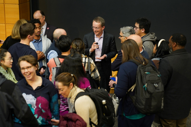
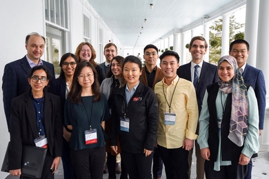
The second annual student-industry conference was held in-person for the first time.
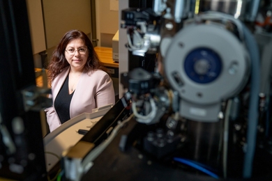
Materials scientist Anna Osherov helps researchers comprehend the nanoscale down to an atom using MIT.nano’s characterization tools.
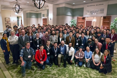
19th Microsystems Annual Research Conference reveals the next era of microsystems technologies, along with skiing and a dance party.