Microsystems Annual Research Conference goes virtual, preserves human touch
Student committee delivers interactive conference on microsystems and nanoscience.
Student committee delivers interactive conference on microsystems and nanoscience.
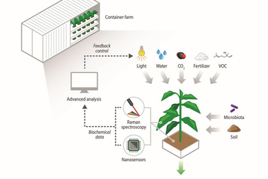
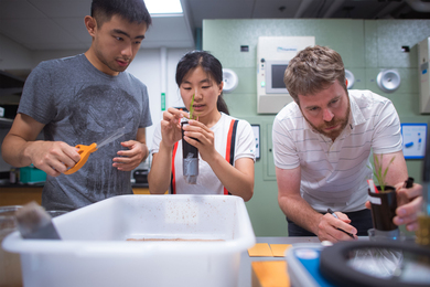
Engineered plant nanosensors and portable Raman spectroscopy will help enable sustainable practices in traditional and urban agriculture.
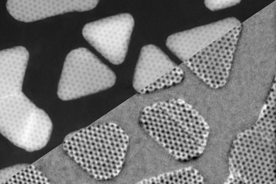
Cutting-edge microscope helps reveal ways to control the electronic properties of atomically thin materials.
Inspired by personal tragedy, graduate student Hyunwoo Yuk used his background in soft materials to develop a bioadhesive tape for repairing damaged tissue.
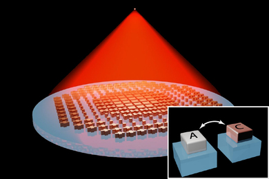
The design may enable miniature zoom lenses for drones, cellphones, or night-vision goggles.
MIT junior faculty explore new research directions and achieve powerful career advancement enabled by J-WAFS’ mission-driven grant program focused on water and food solutions.

The MIT Climate and Sustainability Consortium launches with 13 company members to work with MIT on innovation in climate and sustainability.

Self-assembly of Kevlar-inspired molecules leads to structures with robust properties, offering new materials for solid-state applications.
Manipulating materials at a fundamental level, Ju Li reveals new properties for energy applications.

In two years, the MIT Quest for Intelligence has allowed hundreds of students to explore AI in its many applications.

Faculty members recognized for excellence via a diverse array of honors, grants, and prizes over the past two quarters.
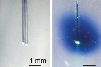
Miniaturized device activates drugs in a small region deep within the brain.
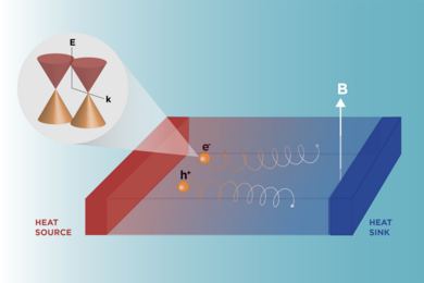
A quantum effect in topological semimetals demonstrated by MIT researchers could allow for the utilization of an untapped energy source.

For senior Danielle Grey-Stewart, a pivotal experience away from campus led to a new sense of purpose at MIT.
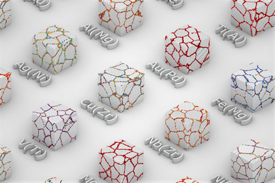
System uses machine learning to analyze boundaries between crystal grains, allowing for selection of desired properties in a new metal.