“Illuminating.” “Spectacular.” “Compelling.” This is how community college students described the two days they spent at MIT.nano learning about the complex tools inside the cleanroom and building and packaging their own functional photonic chips.
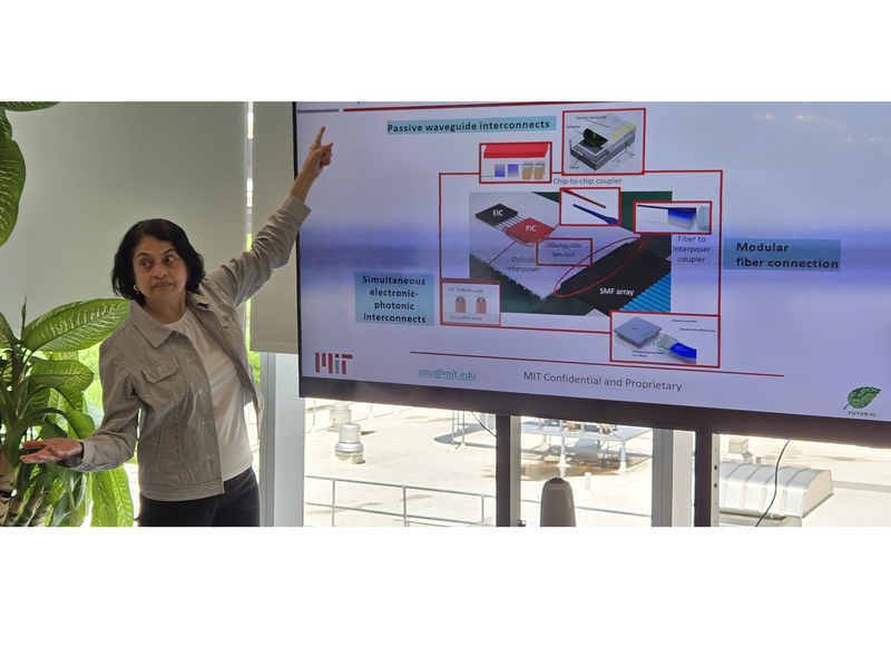
“Integrated photonics is an essential part of semiconductor packaging today,” says Anu Agarwal, principal research scientist in the Materials Research Laboratory at MIT. “But there is no single, standardized university curriculum for integrated electronics-photonics packaging. We need to create educational materials to teach this subject across the talent pipeline from K-12 and beyond, which is exactly what we’re doing at the Initiative for Knowledge and Innovation in Manufacturing (IKIM) and MIT.nano.”
As leader of the Lab for Education and Application Prototypes (LEAP) facility located on MIT.nano’s fifth floor, Agarwal stresses the importance of hands-on learning when studying integrated photonics, the science of guiding and manipulating light on a semiconductor chip. Through the Northeast Consortia for Advanced Integrated Silicon Technologies (NCAIST) program, she’s bringing community and four-year college students to MIT.nano for experimental boot camps that teach how to use semiconductor tools for electronic-photonic packaging and testing.
“Having a workforce skilled in resource-efficient semiconductor manufacturing, including electronic-photonic packaging, is critical to maintain the exponential growth of the chip industry and build national security,” says Agarwal. “MIT.nano, through programs like NCAIST, are helping to train more people in STEM.”
Working closely with AIM Photonics, a U.S. Manufacturing Innovation Institute, NCAIST coordinates and accelerates the transition of technician education content and teaching methodologies from key AIM-affiliated U.S. universities to community, technical, and four-year colleges in the Northeast. Through NCAIST, in Massachusetts, the Massachusetts Bay Community College (MBCC) is paired with MIT, North Shore Community College (NSCC) with Stonehill College, and Springfield Technical Community College (STCC) with Western New England University.
“The NCAIST program offers a transformative opportunity for our community college students to experience hands-on training at MIT.nano’s LEAP facility,” says Marina Bograd, professor and chair of the engineering department at MassBay Community College. “For many of them, this is their first time stepping into a cleanroom or seeing semiconductor manufacturing up close. The experience helps open doors that might otherwise feel out of reach, builds confidence, and inspires our students to see themselves pursuing careers in emerging technologies.”
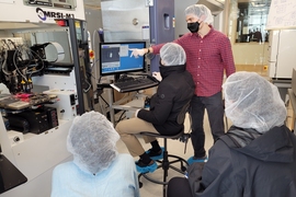
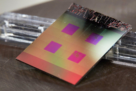
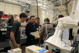
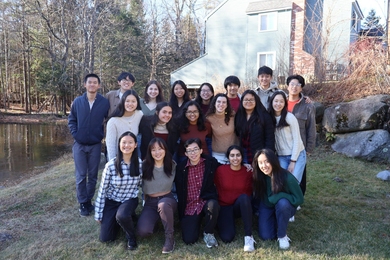
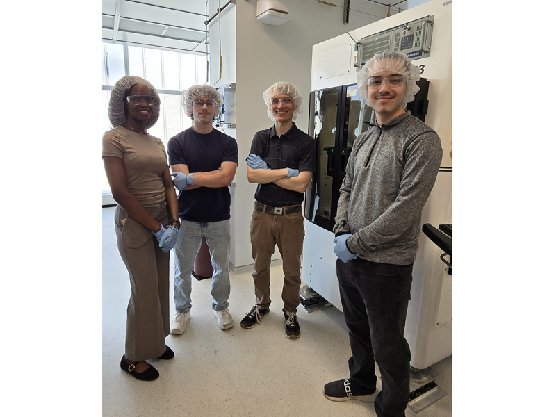
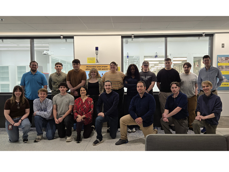
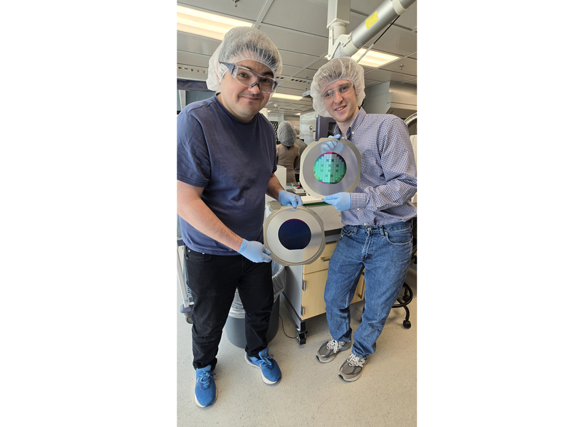
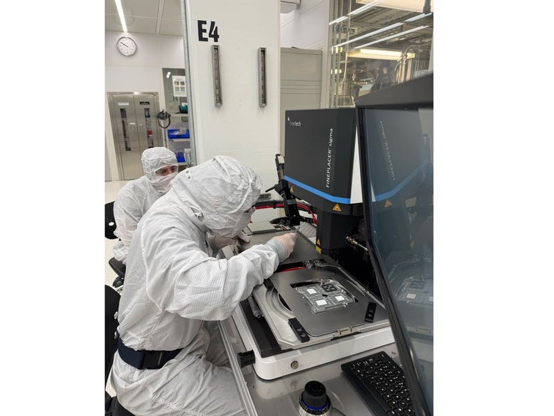
The most recent MIT.nano boot camp, held on May 20-21, expanded participation to include not only those from MBCC, but also students from NSCC, Stonehill College, and SUNY Polytechnic Institute, where NCAIST is headquartered. Twelve students spent two full days at MIT.nano operating a die saw, die bonder, wire bonder, and flip chip tool to build and test a packaged chip.
“I found the combination of hands-on activities, lectures, and informal discussion with the MIT.nano team and fellow students fostered an awesome learning environment,” says Cari Caudill, a student at NSCC. “As a mechanical engineering student, I was most interested in packaging and the machines themselves, so I loved getting direct experience with the tools and discussing with our instructors how procedural and technological development has impacted precision, efficiency, and scalability in the semiconductor industry.”
"The NCAIST boot camp was an exciting and illuminating experience!” adds MassBay Community College student Wyatt Maurer. “I really appreciated getting the chance to work with semiconductor manufacturing tools and to learn about the future of photonics from leaders in the field.”
Students attended lectures on cleanroom safety by Kristofor Payer, assistant director of operations at MIT.nano; electronic-photonic packaging by Agarwal; and photonic integrated circuit sensing by Department of Materials Science and Engineering graduate student Lizzie Gower. They were also offered virtual reality (VR) simulation exercises by Sajan Saini, the director of education at IKIM, to help build intuition about photonic devices and semiconductor packaging tools. These VR simulations serve as a foundational tool to help students visualize photonic devices and complex tool mechanics, as well as run digital process steps and deepen their technical understanding. By bridging physical fabrication with advanced simulation resources, the LEAP students are mastering highly specialized manufacturing, assembly, and testing pipelines required to build the future of electronic-photonic integration.
“The experience at this boot camp not only strengthens our student technical skills, it helps them see themselves as future contributors to a rapidly evolving field,” says Mary Beth Steigerwald, professor and engineering department chair at North Shore Community College. “It also enriches their professional portfolios and gives them a stronger, more compelling story to share during internship and transfer interviews.”
The students will use this training to secure summer internships at hard technology companies. Several have also been accepted to four-year degree programs to continue their education in the fall.