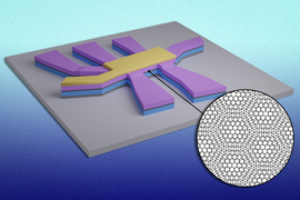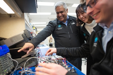
In 2021, a team led by MIT physicists reported creating a new ultrathin ferroelectric material, or one where positive and negative charges separate into different layers. At the time they noted the material’s potential for applications in computer memory and much more. Now the same core team and colleagues — including two from the lab next door — have built a transistor with that material and shown that its properties are so useful that it could change the world of electronics.
Although the team’s results are based on a single transistor in the lab, “in several aspects its properties already meet or exceed industry standards” for the ferroelectric transistors produced today, says Pablo Jarillo-Herrero, the Cecil and Ida Green Professor of Physics, who led the work with professor of physics Raymond Ashoori. Both are also affiliated with the Materials Research Laboratory.
“In my lab we primarily do fundamental physics. This is one of the first, and perhaps most dramatic, examples of how very basic science has led to something that could have a major impact on applications,” Jarillo-Herrero says.
Says Ashoori, “When I think of my whole career in physics, this is the work that I think 10 to 20 years from now could change the world.”
Among the new transistor’s superlative properties:
- It can switch between positive and negative charges — essentially the ones and zeros of digital information — at very high speeds, on nanosecond time scales. (A nanosecond is a billionth of a second.)
- It is extremely tough. After 100 billion switches it still worked with no signs of degradation.
- The material behind the magic is only billionths of a meter thick, one of the thinnest of its kind in the world. That, in turn, could allow for much denser computer memory storage. It could also lead to much more energy-efficient transistors because the voltage required for switching scales with material thickness. (Ultrathin equals ultralow voltages.)
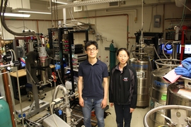
The work is reported in a recent issue of Science. The co-first authors of the paper are Kenji Yasuda, now an assistant professor at Cornell University, and Evan Zalys-Geller, now at Atom Computing. Additional authors are Xirui Wang, an MIT graduate student in physics; Daniel Bennett and Efthimios Kaxiras of Harvard University; Suraj S. Cheema, an assistant professor in MIT’s Department of Electrical Engineering and Computer Science and an affiliate of the Research Laboratory of Electronics; and Kenji Watanabe and Takashi Taniguchi of the National Institute for Materials Science in Japan.
What they did
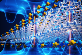
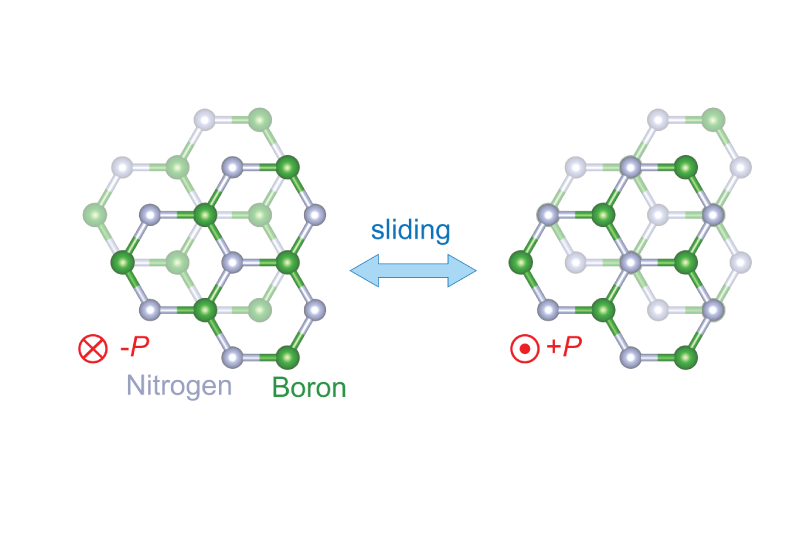
In a ferroelectric material, positive and negative charges spontaneously head to different sides, or poles. Upon the application of an external electric field, those charges switch sides, reversing the polarization. Switching the polarization can be used to encode digital information, and that information will be nonvolatile, or stable over time. It won’t change unless an electric field is applied. For a ferroelectric to have broad application to electronics, all of this needs to happen at room temperature.
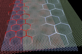
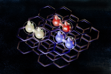
The new ferroelectric material reported in Science in 2021 is based on atomically thin sheets of boron nitride that are stacked parallel to each other, a configuration that doesn’t exist in nature. In bulk boron nitride, the individual layers of boron nitride are instead rotated by 180 degrees.
It turns out that when an electric field is applied to this parallel stacked configuration, one layer of the new boron nitride material slides over the other, slightly changing the positions of the boron and nitrogen atoms. For example, imagine that each of your hands is composed of only one layer of cells. The new phenomenon is akin to pressing your hands together then slightly shifting one above the other.
“So the miracle is that by sliding the two layers a few angstroms, you end up with radically different electronics,” says Ashoori. The diameter of an atom is about 1 angstrom.
Another miracle: “nothing wears out in the sliding,” Ashoori continues. That’s why the new transistor could be switched 100 billion times without degrading. Compare that to the memory in a flash drive made with conventional materials. “Each time you write and erase a flash memory, you get some degradation,” says Ashoori. “Over time, it wears out, which means that you have to use some very sophisticated methods for distributing where you’re reading and writing on the chip.” The new material could make those steps obsolete.
A collaborative effort
Yasuda, the co-first author of the current Science paper, applauds the collaborations involved in the work. Among them, “we [Jarillo-Herrero’s team] made the material and, together with Ray [Ashoori] and [co-first author] Evan [Zalys-Geller], we measured its characteristics in detail. That was very exciting.” Says Ashoori, “many of the techniques in my lab just naturally applied to work that was going on in the lab next door. It’s been a lot of fun.”
Ashoori notes that “there’s a lot of interesting physics behind this” that could be explored. For example, “if you think about the two layers sliding past each other, where does that sliding start?” In addition, says Yasuda, could the ferroelectricity be triggered with something other than electricity, like an optical pulse? And is there a fundamental limit to the amount of switches the material can make?
Challenges remain. For example, the current way of producing the new ferroelectrics is difficult and not conducive to mass manufacturing. “We made a single transistor as a demonstration. If people could grow these materials on the wafer scale, we could create many, many more,” says Yasuda. He notes that different groups are already working to that end.
Concludes Ashoori, “There are a few problems. But if you solve them, this material fits in so many ways into potential future electronics. It’s very exciting.”
This work was supported by the U.S. Army Research Office, the MIT/Microsystems Technology Laboratories Samsung Semiconductor Research Fund, the U.S. National Science Foundation, the Gordon and Betty Moore Foundation, the Ramon Areces Foundation, the Basic Energy Sciences program of the U.S. Department of Energy, the Japan Society for the Promotion of Science, and the Ministry of Education, Culture, Sports, Science and Technology (MEXT) of Japan.