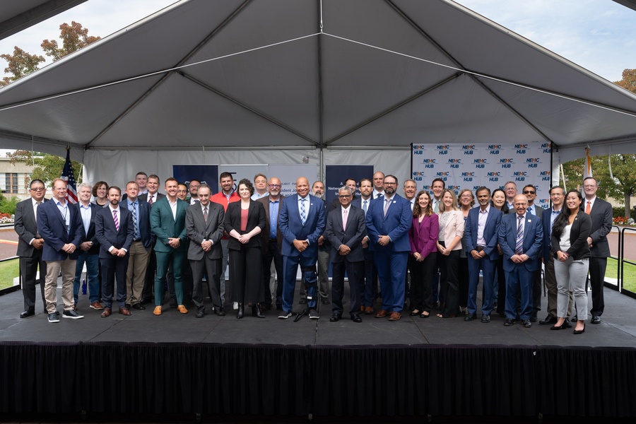
MIT and Lincoln Laboratory are participants in four microelectronics proposals selected for funding to the Northeast Microelectronics Coalition (NEMC) Hub. The funding comes from the Microelectronics Commons, a $2 billion initiative of the CHIPS and Science Act to strengthen U.S. leadership in semiconductor manufacturing and innovation. The regional awards are among 33 projects announced as part of a $269 million federal investment.
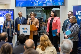
U.S. Department of Defense (DoD) and White House officials announced the awards during an event on Sept. 18, hosted by the NEMC Hub at MIT Lincoln Laboratory. The NEMC Hub, a division of the Massachusetts Technology Collaborative, leads a network of more than 200 member organizations across the region to enable the lab-to-fab transition of critical microelectronics technologies for the DoD. The NEMC Hub is one of eight regional hubs forming a nationwide chip network under the Microelectronics Commons and is executed through the Naval Surface Warfare Center Crane Division and the National Security Technology Accelerator (NSTXL).
"The $38 million in project awards to the NEMC Hub are a recognition of the capability, capacity, and commitment of our members," said Mark Halfman, NEMC Hub director. "We have a tremendous opportunity to grow microelectronics lab-to-fab capabilities across the Northeast region and spur the growth of game-changing technologies."
"We are very pleased to have Lincoln Laboratory be a central part of the vibrant ecosystem that has formed within the Microelectronics Commons program," said Mark Gouker, assistant head of the laboratory's Advanced Technology Division and NEMC Hub advisory group representative. "We have made strong connections to academia, startups, DoD contractors, and commercial sector companies through collaborations with our technical staff and by offering our microelectronics fabrication infrastructure to assist in these projects. We believe this tighter ecosystem will be important to future Microelectronics Commons programs as well as other CHIPS and Science Act programs."
The nearly $38 million award to the NEMC Hub is expected to support six collaborative projects, four of which will involve MIT and/or Lincoln Laboratory.
"These projects promise significant gains in advanced microelectronics technologies," said Ian A. Waitz, MIT's vice president for research. "We look forward to working alongside industry and government organizations in the NEMC Hub to strengthen U.S. microelectronics innovation, workforce and education, and lab-to-fab translation."
The projects selected for funding support key technology areas identified in the federal call for competitive proposals. MIT campus researchers will participate in a project advancing commercial leap-ahead technologies, titled "Advancing DoD High Power Systems: Transition of High Al% AlGaN from Lab to Fab," and another in the area of 5G/6G, called "Wideband, Scalable MIMO arrays for NextG Systems: From Antennas to Decoders."
Researchers both at Lincoln Laboratory and on campus will contribute to a quantum technology project called "Community‐driven Hybrid Integrated Quantum‐Photonic Integrated circuits (CHIQPI)."
Lincoln Laboratory researchers will also participate in the "Wideband Same‐Frequency STAR Array Platform Based on Heterogeneous Multi-Domain Self‐Interference Cancellation" project.
The anticipated funding for these four projects follows a $7.7 million grant awarded earlier this year to MIT from the NEMC Hub, alongside an agreement between MIT and Applied Materials, to add advanced nanofabrication equipment and capabilities to MIT.nano.
The funding comes amid construction of the Compound Semiconductor Laboratory – Microsystem Integration Facility (CSL-MIF) at Lincoln Laboratory. The CSL-MIF will complement Lincoln Laboratory's existing Microelectronics Laboratory, which has remained the U.S. government's most advanced silicon-based research and fabrication facility for decades. When completed in 2028, the CSL-MIF is expected to play a vital role in the greater CHIPS and Science Act ecosystem.
"Lincoln Laboratory has a long history of developing advanced microelectronics to enable critical national security systems," said Melissa Choi, Lincoln Laboratory director. "We are excited to embark on these awarded projects, leveraging our microelectronics facilities and partnering with fellow hub members to be at the forefront of U.S. microelectronics innovation."
Officials who spoke at the Sept. 18 event emphasized the national security and economic imperatives to building a robust microelectronics workforce and innovation network.
"The Microelectronics Commons is an essential part of the CHIPS and Science Act's whole-of-government approach to strengthen the U.S. microelectronics ecosystem and secure lasting technical leadership in this critical sector," said Dev Shenoy, the principal director for microelectronics in the Office of the Under Secretary of Defense for Research and Engineering. "I believe in the incredible impact this work will have for American economies, American defense, and the American people."
"The secret sauce of what made the U.S. the lead innovator in the world for the last 100 years was the coming together of the U.S. government and the public sector, together with the private sector and teaming up with academia and research," said Amos Hochstein, special presidential coordinator for global infrastructure and energy security at the U.S. Department of State. "That is what enabled us to be the forefront of innovation and technology, and that is what we have to do again."


