
Two-dimensional materials, which are only a few atoms thick, can exhibit some incredible properties, such as the ability to carry electric charge extremely efficiently, which could boost the performance of next-generation electronic devices.
But integrating 2D materials into devices and systems like computer chips is notoriously difficult. These ultrathin structures can be damaged by conventional fabrication techniques, which often rely on the use of chemicals, high temperatures, or destructive processes like etching.
To overcome this challenge, researchers from MIT and elsewhere have developed a new technique to integrate 2D materials into devices in a single step while keeping the surfaces of the materials and the resulting interfaces pristine and free from defects.
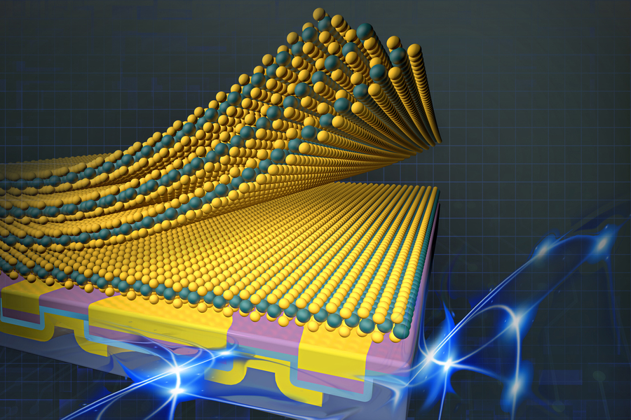
Their method relies on engineering surface forces available at the nanoscale to allow the 2D material to be physically stacked onto other prebuilt device layers. Because the 2D material remains undamaged, the researchers can take full advantage of its unique optical and electrical properties.
They used this approach to fabricate arrays of 2D transistors that achieved new functionalities compared to devices produced using conventional fabrication techniques. Their method, which is versatile enough to be used with many materials, could have diverse applications in high-performance computing, sensing, and flexible electronics.
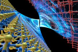
Core to unlocking these new functionalities is the ability to form clean interfaces, held together by special forces that exist between all matter, called van der Waals forces.
However, such van der Waals integration of materials into fully functional devices is not always easy, says Farnaz Niroui, assistant professor of electrical engineering and computer science (EECS), a member of the Research Laboratory of Electronics (RLE), and senior author of a new paper describing the work.
“Van der Waals integration has a fundamental limit,” she explains. “Since these forces depend on the intrinsic properties of the materials, they cannot be readily tuned. As a result, there are some materials that cannot be directly integrated with each other using their van der Waals interactions alone. We have come up with a platform to address this limit to help make van der Waals integration more versatile, to promote the development of 2D-materials-based devices with new and improved functionalities.”
Niroui wrote the paper with lead author Peter Satterthwaite, an electrical engineering and computer science graduate student; Jing Kong, professor of EECS and a member of RLE; and others at MIT, Boston University, National Tsing Hua University in Taiwan, the National Science and Technology Council of Taiwan, and National Cheng Kung University in Taiwan. The research is published today in Nature Electronics.
Advantageous attraction
Making complex systems such as a computer chip with conventional fabrication techniques can get messy. Typically, a rigid material like silicon is chiseled down to the nanoscale, then interfaced with other components like metal electrodes and insulating layers to form an active device. Such processing can cause damage to the materials.
Recently, researchers have focused on building devices and systems from the bottom up, using 2D materials and a process that requires sequential physical stacking. In this approach, rather than using chemical glues or high temperatures to bond a fragile 2D material to a conventional surface like silicon, researchers leverage van der Waals forces to physically integrate a layer of 2D material onto a device.
Van der Waals forces are natural forces of attraction that exist between all matter. For example, a gecko’s feet can stick to the wall temporarily due to van der Waals forces. Though all materials exhibit a van der Waals interaction, depending on the material, the forces are not always strong enough to hold them together. For instance, a popular semiconducting 2D material known as molybdenum disulfide will stick to gold, a metal, but won’t directly transfer to insulators like silicon dioxide by just coming into physical contact with that surface.
However, heterostructures made by integrating semiconductor and insulating layers are key building blocks of an electronic device. Previously, this integration has been enabled by bonding the 2D material to an intermediate layer like gold, then using this intermediate layer to transfer the 2D material onto the insulator, before removing the intermediate layer using chemicals or high temperatures.
Instead of using this sacrificial layer, the MIT researchers embed the low-adhesion insulator in a high-adhesion matrix. This adhesive matrix is what makes the 2D material stick to the embedded low-adhesion surface, providing the forces needed to create a van der Waals interface between the 2D material and the insulator.
Making the matrix
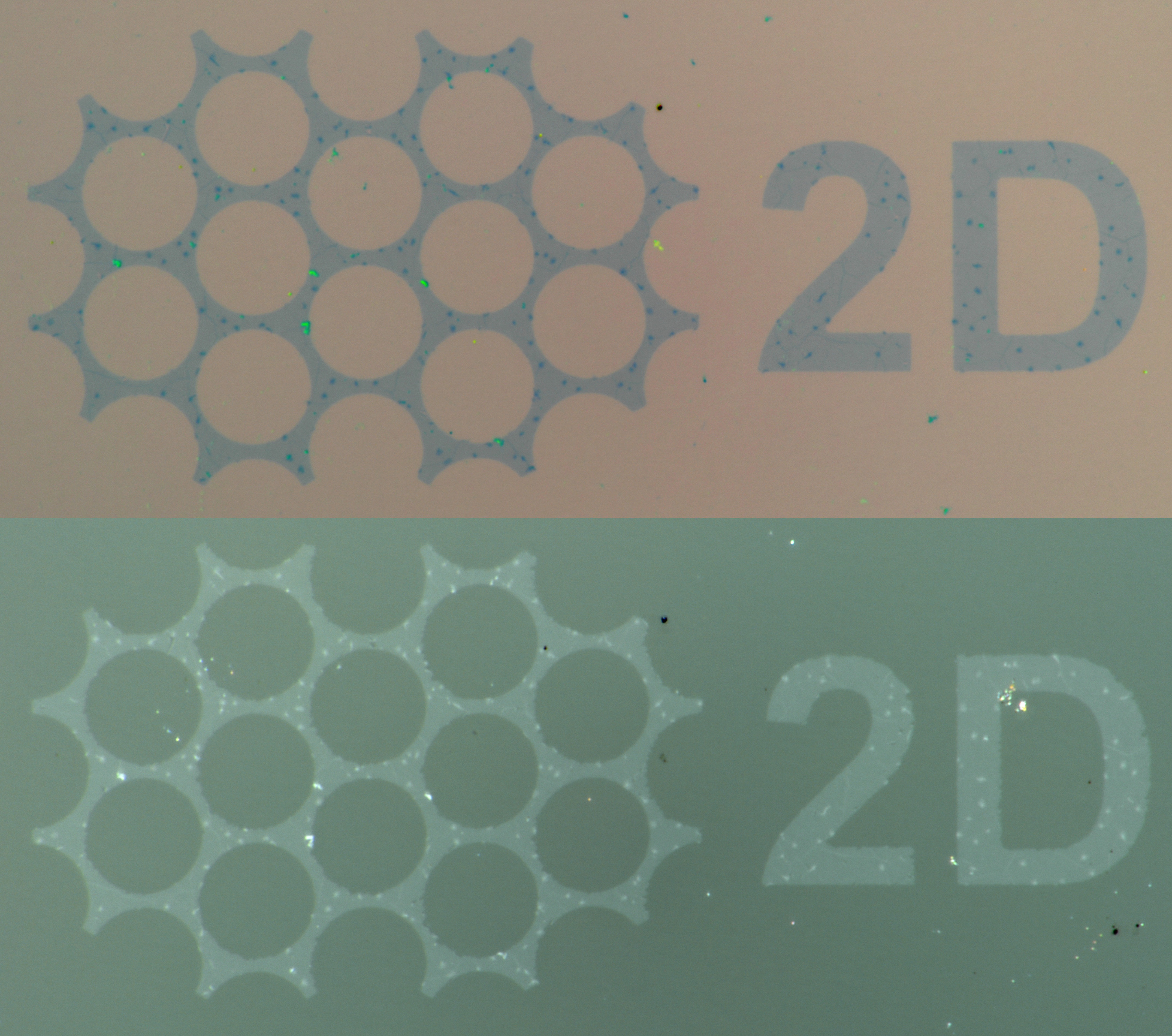
To make electronic devices, they form a hybrid surface of metals and insulators on a carrier substrate. This surface is then peeled off and flipped over to reveal a completely smooth top surface that contains the building blocks of the desired device.
This smoothness is important, since gaps between the surface and 2D material can hamper van der Waals interactions. Then, the researchers prepare the 2D material separately, in a completely clean environment, and bring it into direct contact with the prepared device stack.
“Once the hybrid surface is brought into contact with the 2D layer, without needing any high-temperatures, solvents, or sacrificial layers, it can pick up the 2D layer and integrate it with the surface. This way, we are allowing a van der Waals integration that would be traditionally forbidden, but now is possible and allows formation of fully functioning devices in a single step,” Satterthwaite explains.
This single-step process keeps the 2D material interface completely clean, which enables the material to reach its fundamental limits of performance without being held back by defects or contamination.
And because the surfaces also remain pristine, researchers can engineer the surface of the 2D material to form features or connections to other components. For example, they used this technique to create p-type transistors, which are generally challenging to make with 2D materials. Their transistors have improved on previous studies, and can provide a platform toward studying and achieving the performance needed for practical electronics.
Their approach can be done at scale to make larger arrays of devices. The adhesive matrix technique can also be used with a range of materials, and even with other forces to enhance the versatility of this platform. For instance, the researchers integrated graphene onto a device, forming the desired van der Waals interfaces using a matrix made with a polymer. In this case, adhesion relies on chemical interactions rather than van der Waals forces alone.
In the future, the researchers want to build on this platform to enable integration of a diverse library of 2D materials to study their intrinsic properties without the influence of processing damage, and develop new device platforms that leverage these superior functionalities.
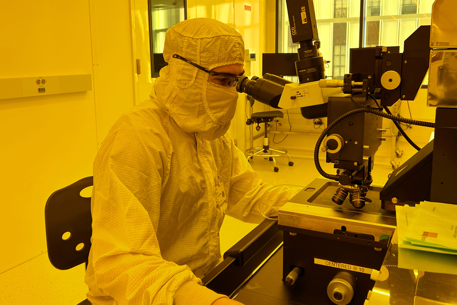
This research is funded, in part, by the U.S. National Science Foundation, the U.S. Department of Energy, the BUnano Cross-Disciplinary Fellowship at Boston University, and the U.S. Army Research Office. The fabrication and characterization procedures were carried out, largely, in the MIT.nano shared facilities.