

Researchers around the world have been working to harness the unusual properties of graphene, a two-dimensional sheet of carbon atoms. But graphene lacks one important characteristic that would make it even more useful: a property called a bandgap, which is essential for making devices such as computer chips and solar cells.
Now, researchers at MIT and Harvard University have found a two-dimensional material whose properties are very similar to graphene, but with some distinct advantages — including the fact that this material naturally has a usable bandgap.
The research, just published online in the Journal of the American Chemical Society, was carried out by MIT assistant professor of chemistry Mircea Dincă and seven co-authors.
The new material, a combination of nickel and an organic compound called HITP, also has the advantage of self-assembly: Its constituents naturally assemble themselves, a “bottom-up” approach that could lend itself to easier manufacturing and tuning of desired properties by adjusting relative amounts of the ingredients.
Research on such two-dimensional materials, which often possess extraordinary properties, is “all the rage these days, and for good reason,” Dincă says. Graphene, for example, has extremely good electrical and thermal conductivity, as well as great strength. But its lack of a bandgap forces researchers to modify it for certain uses — such as by adding other molecules that attach themselves to its structure — measures that tend to degrade the properties that made the material desirable in the first place.
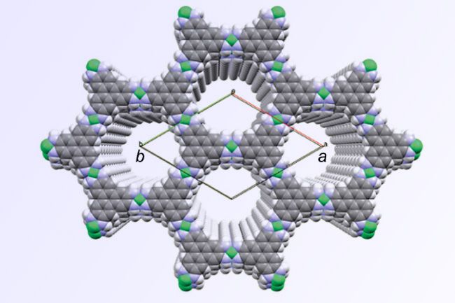
The new compound, Ni3(HITP)2, shares graphene’s perfectly hexagonal honeycomb structure. What’s more, multiple layers of the material naturally form perfectly aligned stacks, with the openings at the centers of the hexagons all of precisely the same size, about 2 nanometers (billionths of a meter) across.
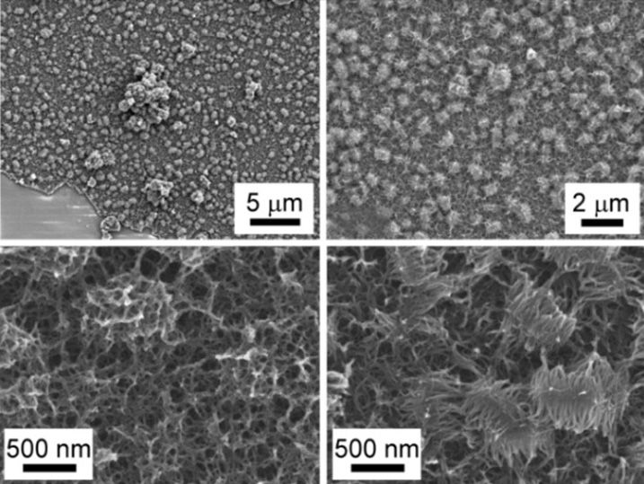
In these initial experiments, the researchers studied the material in bulk form, rather than as flat sheets; Dincă says that makes the current results — including excellent electrical conductivity — even more impressive, since these properties should be better yet in a 2-D version of the material. “There’s every reason to believe that the properties of the particles are worse than those of a sheet,” he says, “but they’re still impressive.”
What’s more, this is just the first of what could be a diverse family of similar materials built from different metals or organic compounds. “Now we have an entire arsenal of organic synthesis and inorganic synthesis,” Dincă says, that could be harnessed to “tune the properties, with atom-like precision and virtually infinite tunability.”
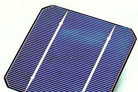
Such materials, Dincă says, might ultimately lend themselves to solar cells whose ability to capture different wavelengths of light could be matched to the solar spectrum, or to improved supercapacitors, which can store electrical energy until it’s needed.
In addition, the new material could lend itself to use in basic research on the properties of matter, or to the creation of exotic materials such as magnetic topological insulators, or materials that exhibit quantum Hall effects. “They’re in the same class of materials that have been predicted to have exotic new electronic states,” Dincă says. “These would be the first examples of these effects in materials made out of organic molecules. People are excited about that.”
Pingyun Feng, a professor of chemistry at the University of California at Riverside who was not involved in this work, says the approach used by this team is “novel and surprising,” and that “the quality of this work, from the synthetic design strategy to the probing of the structural details and to the discovery of exceptional electrical conductivity, is outstanding.” She adds that this finding “represents a major advance in the synthetic design of novel semiconducting materials.”
The work was supported by the U.S. Department of Energy and the Center for Excitonics at MIT.