Lead sulfide nanocrystals suitable for solar cells have a nearly one-to-one ratio of lead to sulfur atoms, but MIT researchers discovered that to make uniformly sized quantum dots, a higher ratio of lead to sulfur precursors – 24 to 1 – is better.
MIT chemical engineering graduate student Mark C. Weidman developed the synthetic recipe in the lab of William A. Tisdale, the Charles and Hilda Roddey Career Development Professor in Chemical Engineering at MIT, with colleagues Ferry Prins, Rachel S. Hoffman and 2013 Summer Scholar Megan Beck. Uniformity of size can promote long exciton diffusion lengths in lead sulfide (PbS) quantum-dot films, Weidman says.
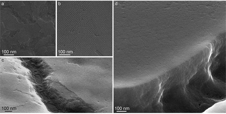
Usually quantum dots are synthesized as a colloid, with particles suspended in a liquid. If the quantum dots are all of the same size, they can self-assemble into an ordered lattice. “If they are monodisperse enough, it’s the thermodynamically favored state,” Weidman explains.
He confirmed the monodispersity of his films with transmission-electron and scanning-electron microscopy. Weidman also traveled to the National Synchrotron Light Source at Brookhaven National Laboratory on Long Island, N.Y., to perform grazing-incidence small-angle X-ray scattering (GISAXS) and wide-angle X-ray scattering (WAXS) studies of his thin films.
“Mark and Megan were able to make extremely monodisperse, unprecedented monodispersity in this particular type of nanocrystal, lead sulfide,” Tisdale says. Weidman unraveled the mechanism for the uniform size and structure.
Weidman, who expects to finish his PhD at MIT in 2016, is interested in lead sulfide because of its uses for solar cells. “In something like a lead sulfide film which is used for photovoltaics, for solar cells, in that case you want your quantum dots to absorb light. But then you don’t want it to re-emit. You want to take that electron and hole and basically get them out of the film, get them to an external circuit. So, you want to maximize diffusion in your film; you want it to be very easy to withdraw this electron and hole pair and you want a long lifetime of that electron and hole pair so you have a lot of time for it to wander around the film and get extracted,” Weidman says.
“We’re hoping to find ways to better increase the efficiency of solar cells by making your diffusion lengths in films of lead sulfide much longer, and that way it's easier to extract charge carriers from the film.”
Diffusion length refers to the process of excitons (pairs of oppositely charged electrons and holes) moving, or “hopping,” from quantum dot to quantum dot, or from quantum dots to a neighboring material. Both the distance excitons travel and their lifetime affect potential applications. Weidman was a co-author of a collaborative study among professors Tisdale, Vladimir Bulovic, and Adam Willard of diffusion in quantum dot solids, which measured exciton lifetimes and modeled exciton diffusion lengths. Fellow graduate student A. Jolene Mork assisted in sample preparation and in transient spectroscopy measurements.
For that study, Weidman performed electron microscopy and analysis using image-processing tools and MATLAB programming to determine the separation, or physical distance, between quantum dots in the film. The cadmium selenide core quantum dots with a cadmium zinc sulfur shell averaged center-to-center distances of about 7.9 nanometers apart. “What we learned is you want to make the center-to-center distance as small as possible to have a longer diffusion length, to maximize your diffusion length,” Weidman says.
Quantum dots are also valued for their property of changing color as they change size, which is tied to their changing bandgap. To have a consistent color, you have to have a consistent size among an ensemble of quantum dots. Tisdale group colleague Elizabeth M.Y. (Liza) Lee did simulated size variations in the quantum-dot film for the study, Weidman notes. “This paper is pretty much showing that you can control how much energetic diffusion occurs in films of quantum dots by tailoring how close they are physically,” he explains.
“The other big implication in this paper is that from what we saw in some of the simulations, some energetic disorder can be good in these films in order to get the ball rolling on energy diffusion. If you have some size variations and that gives you energy variations, then when you excite this film, and you get this population of excited quantum dots, then some of them are higher energy than others, some of them are lower energies, so naturally the excitons that are on the higher-energy quantum dots will find the lower-energy site, and that’s energy diffusion. So a little bit of size variation can help to speed up that process,” Weidman says. “If you think about it as a hilly landscape, you have these excitons that are at the top of hill, and they find a way to roll down to the bottom of hill, whereas if you had a completely homogeneous film that is flat in energy, then you don’t start energy diffusion as quickly.”
Weidman is lead author a Chemistry of Materials paper that further investigated and characterized the superlattice formation of lead sulfide nanocrystals. “We can make long-range superlattices in which not only are the quantum dots ordered, but their atomic planes are aligned as well,” Weidman explains. “We also found that we can change the ligand species on the surface of our quantum dots, a great way of modifying the film properties, to more compact and functional species without disturbing the superlattice arrangement.” He currently is investigating transporting energy over long distances in infrared materials, which could be applicable to solar cells.
Weidman, a 26-year-old graduate of the University of Delaware, hails originally from Haddonfield, N.J. After completing his doctorate at MIT, he plans to get a job in industry. “I would like to keep working with nanomaterials,” he says. “I think it’s a very exciting area.”