Material could bring optical communication onto silicon chips
Ultrathin films of a semiconductor that emits and detects light can be stacked on top of silicon wafers.
Ultrathin films of a semiconductor that emits and detects light can be stacked on top of silicon wafers.

Materials Processing Center, Center for Materials Science and Engineering merger brings together formidable resources for advancing next-generation materials.

Researchers demonstrate nanoscale particles that ordinary light sources can set spinning.

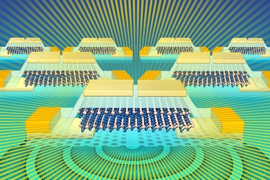
Neural networks could be implemented more quickly using new photonic technology.
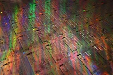
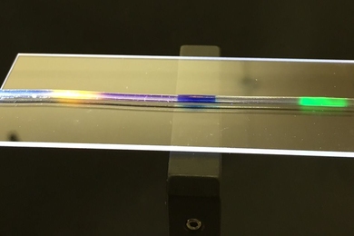
Study: Silicon can reproduce physical phenomena exploited by high-end telecommunications devices.

AIM Photonics fall meeting attendees tackle plans for making computer chips with integrated optical devices and developing a regional workforce.

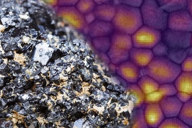
Exotic materials called photonic crystals reveal their internal characteristics with new method.
![“…[I]f a fluorescence microscope’s resolution is set at 2 micrometers, our technique can have 300 nanometer resolution — about a sixfold improvement over regular microscopes,” says MIT graduate student Frederick Sangyeon Cho. “The idea is very simple but very powerful and can be useful in many different imaging applications.”](/sites/default/files/styles/term_page__news_article/public/images/201611/MIT-Laser-Particles.jpg?itok=6w5kR_BC)
New imaging technique stimulates particles to emit laser light, could create higher-resolution images.
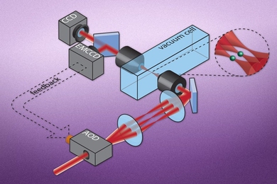
Technique may enable large-scale atom arrays for quantum computing.
MIT researchers use an optical technique to probe magnetism at a hidden interface between two exotic thin films.
Biocompatible fibers could use light to stimulate cells or sense signs of disease.
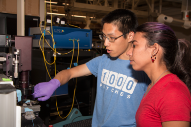
Summer Scholar Ashley Del Valle Morales probes new a silicon carbide system in the MIT Microphotonics Center.

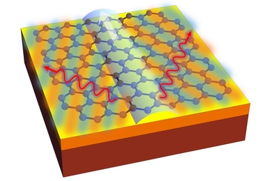
Some “forbidden” light emissions are in fact possible, could enable new sensors and light-emitting devices.
By slowing down light to a speed slower than flowing electrons, researchers create a kind of optical “sonic boom.”
Defects in some new electronic materials can be removed by making ions move under illumination.