New lightweight polymer film can prevent corrosion
Because it’s nearly impermeable to gases, the polymer coating developed by MIT engineers could be used to protect solar panels, machinery, infrastructure, and more.
Because it’s nearly impermeable to gases, the polymer coating developed by MIT engineers could be used to protect solar panels, machinery, infrastructure, and more.

MIT researchers created microscopic wireless electronic devices that travel through blood and implant in target brain regions, where they provide electrical stimulation.

The DIGIT imaging tool could enable the design of quantum devices and shed light on atomic-scale processes in cells and tissues.
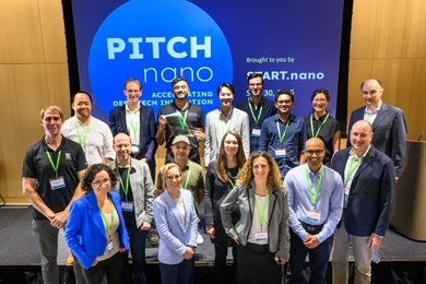
Twelve START.nano companies competed for the grand prize of nanoBucks to be used at MIT.nano’s facilities.

Incorporating machine learning, MIT engineers developed a way to 3D print alloys that are much stronger than conventionally manufactured versions.

Panel discussions focused on innovation in many forms of energy, then a tour of campus featured student research.

The new “CRESt” platform could help find solutions to real-world energy problems that have plagued the materials science and engineering community for decades.

A new device concept opens the door to compact, high-performance transistors with built-in memory.
New findings could provide a way to monitor batteries for sounds that could guide manufacturing, indicate remaining usable life, or flag potential safety issues.

By directly imaging material failure in 3D, this real-time technique could help scientists improve reactor safety and longevity.

The Initiative for New Manufacturing is convening experts across the Institute to drive a transformation of production across the U.S. and the world.

New microparticles containing iron or iodine could be used to fortify food and beverages, to help fight malnutrition.

Nanophotonic devices developed at MIT are compact, efficient, reprogrammable, adaptive, and able to dynamically respond to external inputs.

Device Research Lab study uncovers mechanisms behind a phenomenon that can impact civil engineering, desalination, coatings, membrane design, art conservation, and more.
The new implant carries a reservoir of glucagon that can be stored under the skin and deployed during an emergency — with no injections needed.