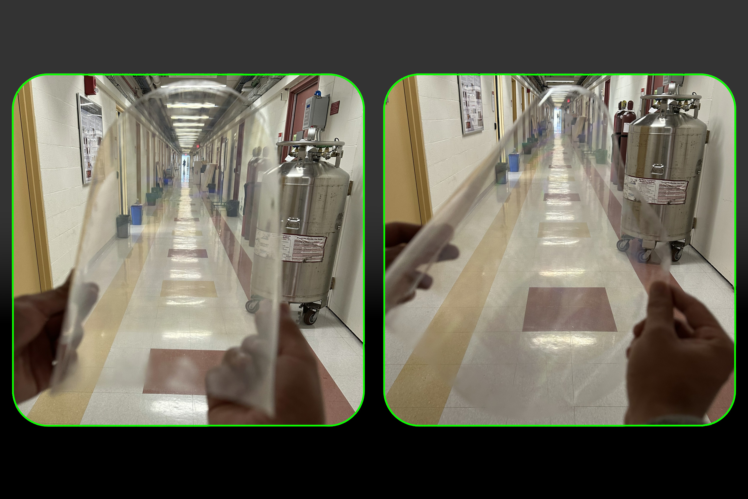
The field of silicon photonics, which uses light rather than electricity to transmit and process data on semiconductor chips, has enabled optical systems to evolve from bulky setups to compact and advanced systems. Typically, however, these silicon-photonics chips are rigid and opaque.
MIT scientists have now figured out a scalable way to make silicon-photonics chips flexible and transparent, opening a route to advanced microchips that could be used in applications such as discreet health monitors that conform to the body or transparent augmented-reality displays that fit the curve of a pilot’s helmet.
While scientists have recently performed lab demonstrations of chips that were flexible or transparent, they could only fabricate a few devices at a time.
The MIT researchers, in close collaboration with engineers at NY Creates at the Albany NanoTech Complex, created a fabrication process that uses standard semiconductor manufacturing techniques to generate flexible and transparent silicon-photonics chips on large-scale wafers.
To validate this platform, the researchers bent a single chip thousands of times around cylinders with various diameters — down to the width of a small screw — with no drop in performance. They also determined that looking through the chips would not cause much haze or distortion.
“We’ve now developed a wafer-scale process that produces wafers that are mechanically flexible and optically transparent, enabling novel applications that weren’t previously possible with silicon photonics. We hope that, by working closely with our colleagues at NY Creates and using the foundry at the Albany NanoTech Complex, there’s the potential for us to make the platform accessible to other groups within our research community and open these new application areas to the field of silicon photonics as a whole,” says Jelena Notaros, the Robert J. Shillman Career Development Associate Professor of Electrical Engineering and Computer Science (EECS) at MIT, a member of the Research Laboratory of Electronics, and senior author of a paper on this fabrication platform.
Her co-authors include lead author Tal Sneh and Andres Garcia Coleto, EECS graduate students; Thomas Dyer and Kevin Fealey of the New York Center for Research, Economic Advancement, Technology, Engineering, and Science (NY Creates); and Milica Notaros PhD ’23. The paper appears in the journal Optica.
Flexible and transparent
Over the past decade, researchers have developed techniques to fabricate precise and highly reliable silicon-photonics devices at scale.
They use advanced microelectronics foundry processes to produce 300-millimeter-diameter wafers with billions of nanoscale optical devices. But these methods yield silicon-photonics chips that are rigid and opaque.
“We realized that there are a lot of applications that would benefit from having a chip that is flexible and transparent,” Notaros says.
Scientists have previously made single silicon-photonics chips that were either transparent or flexible, but these techniques weren’t scalable. To address this scaling challenge, Notaros’ group recently demonstrated a foundry-scale process for making silicon-photonics chips on a flexible substrate.
Now, the team pushed these innovations even farther with a scalable process that produces 300-millimeter silicon-photonics wafers that are both transparent and flexible.
Their fabrication process begins as if they were making a traditional, rigid silicon wafer. The researchers carefully deposit and pattern tiny optical wires known as waveguides onto this rigid silicon substrate.
Then they bond a temporary silicon wafer on top. They flip the wafer over and remove all of the original silicon substrate from what is now the top of the wafer. They are then left with a flat layer of material with a thickness less than a tenth of a human hair.
“Thanks to the fact that we added that rigid temporary support before we flipped the wafer over, we can go all the way down so we are just left with the oxide and waveguiding layers,” Sneh says.
They use an adhesive to stick a thin, transparent polyester film on top of these ultrathin layers and “de-bond” the temporary silicon wafer from the bottom to remove it.
This leaves them with a flexible, transparent wafer only a few microns thick that contains the oxide and waveguide layers needed to capture and transport light for silicon photonics.
“Because we are using stable 300-millimeter foundry fabrication tools, we can design systems with a very large number of devices and feel confident that they are going to perform up to specifications, which is extremely important,” Sneh adds.
The biggest challenge in developing this fabrication process was removing enough material from a large 300-millimeter-diameter silicon wafer to leave only a few microns of material behind.
During fabrication, stress on the wafer typically causes it to bow slightly, making this silicon removal process especially challenging.
“As we were flipping the wafers over on these substrates, if the strain isn’t properly managed and the wafer isn’t perfectly flat, it is going to get ripples across its surface or even shatter in the fabrication line,” Dyer says.
The researchers carefully managed that stress by sticking to low temperature processes at or below 500 degrees Celsius.
They also had to find the right ordering and combination of removal methods.
They used industrial processes to thin the silicon layer, but switched to a more precise selective chemical etch for the last bit. This ensured they would not damage the ultrathin layers left behind.
An eye on performance
The researchers performed three experiments to test different functionalities of these flexible, transparent silicon-photonics wafers.
First, they tested the optical performance of chips with integrated waveguides of different lengths to determine their waveguiding properties.
Then they tested flexibility by bending a chip thousands of times around cylinders with different diameters. These experiments showed no degradation in performance even when they bent it around a cylinder about the size of a small screw. The device didn’t start to degrade until the researchers bent it around a toothpick several times.
“This experiment validated that the platform can be used for our proposed applications, performing even well beyond the metrics required for these intended systems,” Garcia Coleto says.
They also evaluated transparency by setting up a bionic eye and testing whether the chip would distort the user’s vision when placed in front of the eye. They found that the chip causes only minimal haze for the viewer and would not noticeably distort images the eye perceives when looking through it.
These characteristics could make these chips especially well-suited for enabling silicon-photonics systems for applications like curved augmented-reality displays that conform to a heads-up-display windshield or airplane pilot’s visor. In a pilot’s visor, for instance, such an augmented-reality display could replace the heavy bulk-optical systems that currently provide real-time information to help the pilot react to dangerous conditions.
In the future, the researchers want to add more complex components and functionality to the chips as they move toward enabling these and other new applications. They also want to refine the design to further improve waveguide efficiency and boost transparency performance.
This research was funded, in part, by the National Science Foundation, the U.S. Defense Advanced Research Projects Agency, and a MathWorks Fellowship. Wafer processing was performed at NY Creates, and chip dicing was conducted at MIT.nano.