Although silicon is the workhorse of the semiconductor industry, forming the basis for computer chips, camera sensors, and other everyday electronic devices, researchers and manufacturers add other materials, such as germanium, to boost silicon chip processing speed, cut power consumption, and create new functions, such as photonic connections that use light instead of electrical current to transfer data.
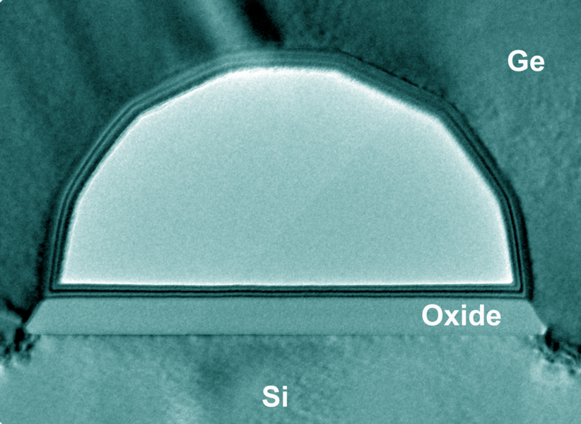
Researchers have known for about a decade that dome-shaped empty spaces form in germanium when it is grown on top of silicon patterned with a dielectric material, such as silicon oxide or silicon nitride, that masks part of the silicon base. Now, MIT researchers have discovered a method to predict and control the length of tunnels in solid germanium by growing it on silicon oxide strips on top of silicon. These tunnels have potential to be used as light channels for silicon photonics or liquid channels for microfluidic devices.
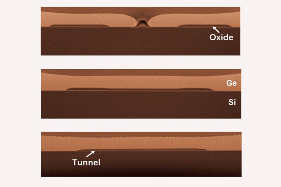
“We found a tunnel or cavity on top of the silicon dioxide which is between the germanium and the silicon dioxide, and we can vary the length of the tunnel depending on the length of the oxide,” says Rui-Tao Wen, a former MIT postdoc and first author of a recent paper in Nano Letters. Wen is now an assistant professor of materials science and engineering at the Southern University of Science and Technology in Shenzhen, China.
The researchers used a two-step growth process, which first puts down a layer of germanium at a relatively lower temperature, then adds another germanium layer at a relatively higher temperature. The germanium layers have difficulty bonding directly to the silicon oxide strips. “The major discovery was that you form these cavities or tunnels, and they’re actually reconfiguring during growth or annealing,” says Jurgen Michel, Materials Research Laboratory senior research scientist and senior lecturer in the Department of Materials Science and Engineering. “The reconfiguration internally is a basic scientific phenomenon that I don’t think anybody would have expected.”
Evolving over time
During their experiments, which took a year to carry out, first author Wen analyzed cross-sections of the germanium-silicon oxide material with a transmission electron microscope (TEM), capturing images at multiple points in time during its formation. Before actually analyzing their results, the researchers expected that once tunnels formed they would stay the same shape throughout the process. Instead, they found a large amount of material is reconfigured within that space as the material evolves over time. “This is something that nobody has observed yet, that you can actually get this, what we call internal reconfiguration of material,” Michel says.
“So for instance, the tunnel gets larger, some of the connected material completely disappears, and the tunnel surfaces are perfect in terms that they are atomically flat,” Michel says. “They form actually what are called facets, which are certain crystallographic germanium orientations.”
The fine resolution that Wen obtained with TEM images unexpectedly showed these internal surfaces appear to have perfect surfaces. “Normally, if we do epitaxial growth of germanium on silicon, we will find very many dislocations,” Wen says. “There are none of those defects on top of the tunnels. It’s not like materials we used to have, which have a lot of dislocations in germanium layers. This one is a perfect single crystal.” Co-author Baoming Wang prepared the TEM samples. Wang is a postdoc in Professor Carl V. Thompson’s Materials for Micro and Nano Systems research group.
During the growth process, which is called selective epitaxy growth, a gas containing a compound of germanium and hydrogen (germane) flows into an ultra-high vacuum chemical vapor deposition chamber. At first, the germanium deposits on the silicon, then it slowly overgrows the silicon oxide strips, forming an archway-shaped tunnel centered directly over the oxide strips.
Wen patterned silicon oxide strips up to 2 centimeters in length (about three-quarters of an inch) on a 6-inch (about 15 cm) silicon wafer with tunnels covering the entire length of the strip. The strips themselves ranged in size from a width of 350 to 750 nanometers and lengths of 2 microns to 2 cm. The only limit to tunnel length appears to be the size of the silicon base layer, Michel suggests. “We see that the ends of that strip are partially covered with germanium, but then the tunnel length increases with strip length. And that’s a linear process,” he says.
Growth conditions
In these experiments, the pressure in the tunnels was about 10 millibars, which is about 100 times weaker than sea-level atmospheric pressure. Suggesting a mechanism for how the tunnels form, Michel explains that the germanium cannot form a stable germanium oxide directly on top of the silicon oxide in the high temperature, ultra-high vacuum environment, so the process slowly consumes the oxide. “You lose some of the oxide thickness during growth, but the area will stay clear,” he says. Rather than being empty, the tunnels are likely occupied by hydrogen gas, which is present because the germane gas separates into its germanium and hydrogen components.
Another surprising finding was that as the germanium spreads over the silicon oxide strips, it does so unevenly at first, covering the far ends of the strip and then moving toward the centers of the strips. But as this process continues, the uncovered area of the silicon oxide shrinks from an oval shape to a circle, after which the germanium evenly spreads over the remaining uncovered area.
“The effect of the length of the oxide stripe on tunnel formation is surprising and deserves further explanation, both for theoretical understanding and for possible applications,” says Ted Kamins, an adjunct professor of electrical engineering at Stanford University, who was not involved in this research. “The end effects might be useful for introducing liquids or gases into the tunnels. Overgrowth only from the ends of the oxide stripe is also unexpected for four-fold symmetric materials, such as Si (silicon) and Ge (germanium).”
“If controllable and reproducible, the technique might be applied to photonics, where an abrupt change of refractive index can help guide light, and to microfluidics integrated onto a silicon chip,” Kamins says.
“The results are absolutely fascinating and shocking — my jaw drops when going through the electron microscopy photos,” says Jifeng Liu, an associate professor of engineering at Dartmouth College, who was not involved in this research. “Imagine all the pillars in the middle of the Longfellow Bridge gradually and spontaneously migrate to the banks, and one day you find the entire bridge completely suspended in the middle! This would be analogous to what has been reported in this paper on microscopic scale.”
As a postdoc at MIT from 2007 to 2010, Liu worked on the first germanium laser and the first germanium-silicon electroabsorption modulator with Jurgen Michel and Lionel C. Kimerling, the Thomas Lord Professor of Materials Science and Engineering. At Dartmouth, Liu continues research on germanium and other materials such as germanium-tin compounds for photonic integration on silicon platforms.
“I hope these beautiful and shocking results also remind all of us about the central importance of hands-on experimental research and training, even in an emerging age of artificial intelligence and machine learning — you simply cannot calculate and predict everything, not even in a material growth process that has been studied for three decades,” Liu says.
Kamins notes that “This experimental study produced a significant amount of data that should be used to gain an understanding of the mechanisms. Then, the technique can be assessed for its practicality for applications.”
Michel notes that the although the findings about tunnel formation were demonstrated in a specific growth system of germanium on silicon using silicon oxide to pattern growth, these results also should apply to similar growth systems based on combinations of elements such as aluminum, gallium, and arsenic or indium and phosphorus that are called III-V semiconductor materials. “Any kind of growth system where you have this selective growth, you should be able to generate tunnels and voids,” Michel says.
Additional experiments will need to be carried out to see if this process can produce devices for microfluidics, photonics, or possibly passing light and liquid through together. “It’s a very first step toward applications,” Michel says.
This research was supported by the National Science Foundation.

