Exotic 2-D materials hold great promise for creating atom-thin circuits that could power flexible electronics, optoelectronics, and other next-generation devices. But fabricating complex 2-D circuits requires multiple time-consuming, expensive steps.
In a paper published in PNAS, researchers from MIT and elsewhere describe a technique that streamlines the fabrication process, by growing a 2-D material directly onto a patterned substrate and recycling the circuit patterns.
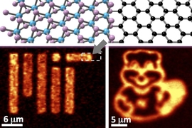
The researchers carefully grow a single layer of molybdenum disulfide (MoS2), which is just three atoms thick, onto a growth substrate in a chosen pattern. This approach differs from traditional techniques that grow and etch away a material iteratively, over multiple layers. Those processes take a while and increase the chances of causing surface defects that may hinder the performance of the material.
With the new method, using only water, the researchers can transfer the material from its growth substrate to its destination substrate so cleanly that the original patterned substrate can be reused as a “master-replica” type of mold — meaning a reusable template for manufacturing. In traditional fabrication, growth substrates get tossed after each material transfer, and the circuit must be patterned again on a new substrate to regrow more material.
“When we scale up and make more complex electronic devices, people need to integrate numerous 2-D materials into more layers and specific shapes. If we follow traditional methods, step by step, it will be very time consuming and inefficient,” says the first author Yunfan Guo, a postdoc in the Department of Electrical Engineering and Computer Science (EECS) and the Research Laboratory of Electronics. “Our method shows the potential to make the whole fabrication process simpler, lower cost, and more efficient.”
In their work, the researchers fabricated arbitrary patterns and a working transistor made from MoS2, which is one of the thinnest known semiconductors. In their study, the researchers recycled the same patterned substrate four times without seeing signs of wear.
Guo is joined on the paper by EECS professor Jing Kong; Professor Xi Ling of Boston University; EECS professor Tomas Palacios; Ju Li, an MIT professor of nuclear science and engineering and of materials science and engineering; Professor David Mullar of Cornell University; Professor Letian Dou of Purdue University; and by seven other MIT graduate students and postdocs; and two other co-authors from Cornell University and Purdue University.
Controlled growth
To design a pattern on a growth substrate, the researchers leveraged a technique that uses oxygen-based plasma to carve patterns into a substrate’s surface. Some version of this technique has been used experimentally before to grow 2-D material patterns. But the spatial resolution — meaning the size of precise structures that can be fabricated — is relatively poor (100 microns), and the electrical performance has been much lower than materials grown using other methods.
To fix this, the researchers conducted in-depth studies into how MoS2 atoms arrange themselves on a substrate surface and how certain chemical precursors can help control the material’s growth. In doing so, they were able to leverage the technique to grow a single layer of high-quality MoS2 within precise patterns.
The researchers used traditional photolithography masks on a silicon oxide substrate, where the desired pattern lies within regions unexposed to light. Those regions are subsequently exposed to the oxygen-based plasma. The plasma etches away about 1-2 nanometers of the substrate in the pattern.
This process also creates a higher surface energy and an enhanced affinity for water-loving (“hydrophilic”) molecules in these plasma-treated regions. The researchers then use an organic salt, called PTAS, that acts as a growth promoter for MoS2. The salt is attracted to the newly created hydrophilic etched regions. In addition, the researchers used sulfur, an essential precursor for MoS2 growth, at a precise amount and temperature to regulate exactly how many of the material’s atoms will form on the substrate.
When the researchers subsequently measured the MoS2 growth, they found it filled in about 0.7 nanometers of the etched pattern. That’s equivalent to exactly one layer of MoS2.
Recycled patterns
Next, the researchers developed a method to recycle the patterned substrate. Traditionally, transferring 2-D materials from a growth substrate onto a destination substrate, such as a flexible surface, requires encasing the whole grown material in a polymer, chemically etching it, and separating it from its growth substrate. But this inevitably brings in contaminants to the material. When the material released, it also leaves behind residue, so the original substrates may not be reused.
Due to the weak interaction between MoS2 and the growth substrate, however, the researchers found they could detach the MoS2 cleanly from the original substrate by submerging it in water. This process, called “delamination,” eliminates the need for using any supporting layer and produces a clean break with the material from the substrate.
“That’s why we can recycle it,” Guo says. “After it’s transferred, because it is purely clean, our patterned substrate is recovered and we can use it for multiple growths.”
The researchers’ innovations introduce far fewer surface defects that limit performance, as measured in electron mobility — how fast electrons move through a semiconductor.
In their paper, the researchers fabricated a 2-D transistor, called a field-effect transistor. Results indicate the electron mobility and “on-off ratio” — how efficiently a transistor flicks between the 1 and 0 computational states — are comparable with the reported values of traditionally grown high-quality, high-performance materials.
The field-effect transistor currently has a spatial resolution of about 2 microns, which is limited only by the laser the microfabrication instruments the researchers used. Next, the researchers hope to shrink the pattern size, and directly integrate complex circuits on 2-D materials using their fabrication technique.