A variety of two-dimensional materials that have promising properties for optical, electronic, or optoelectronic applications have been held back by the fact that they quickly degrade when exposed to oxygen and water vapor. The protective coatings developed thus far have proven to be expensive and toxic, and cannot be taken off.
Now, a team of researchers at MIT and elsewhere has developed an ultrathin coating that is inexpensive, simple to apply, and can be removed by applying certain acids.
The new coating could open up a wide variety of potential applications for these “fascinating” 2D materials, the researchers say. Their findings are reported this week in the journal PNAS, in a paper by MIT graduate student Cong Su; professors Ju Li, Jing Kong, Mircea Dinca, and Juejun Hu; and 13 others at MIT and in Australia, China, Denmark, Japan, and the U.K.
Research on 2D materials, which form thin sheets just one or a few atoms thick, is “a very active field,” Li says. Because of their unusual electronic and optical properties, these materials have promising applications, such as highly sensitive light detectors. But many of them, including black phosphorus and a whole category of materials known as transition metal dichalcogenides (TMDs), corrode when exposed to humid air or to various chemicals. Many of them degrade significantly in just hours, precluding their usefulness for real-world applications.
“It’s a key issue” for the development of such materials, Li says. “If you cannot stabilize them in air, their processability and usefulness is limited.” One reason silicon has become such a ubiquitous material for electronic devices, he says, is because it naturally forms a protective layer of silicon dioxide on its surface when exposed to air, preventing further degradation of the surface. But that’s more difficult with these atomically thin materials, whose total thickness could be even less than the silicon dioxide protective layer.
There have been attempts to coat various 2D materials with a protective barrier, but so far they have had serious limitations. Most coatings are much thicker than the 2D materials themselves. Most are also very brittle, easily forming cracks that let through the corroding liquid or vapor, and many are also quite toxic, creating problems with handling and disposal.
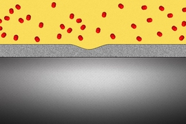
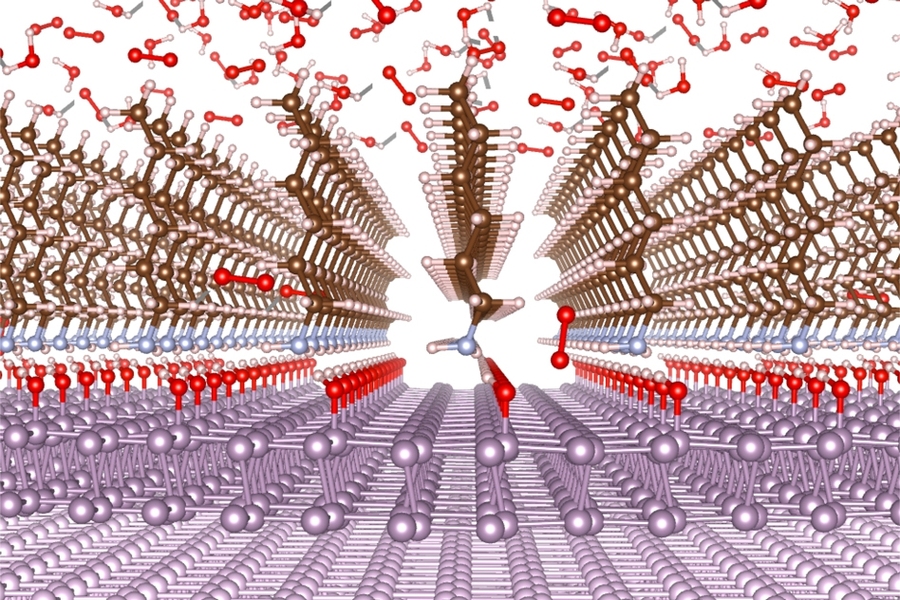
The new coating, based on a family of compounds known as linear alkylamines, improves on these drawbacks, the researchers say. The material can be applied in ultrathin layers, as little as 1 nanometer (a billionth of a meter) thick, and further heating of the material after application heals tiny cracks to form a contiguous barrier. The coating is not only impervious to a variety of liquids and solvents but also significantly blocks the penetration of oxygen. And, it can be removed later if needed by certain organic acids.
“This is a unique approach” to protecting thin atomic sheets, Li says, that produces an extra layer just a single molecule thick, known as a monolayer, that provides remarkably durable protection. “This gives the material a factor of 100 longer lifetime,” he says, extending the processability and usability of some of these materials from a few hours up to months. And the coating compound is “very cheap and easy to apply,” he adds.
In addition to theoretical modeling of the molecular behavior of these coatings, the team made a working photodetector from flakes of TMD material protected with the new coating, as a proof of concept. The coating material is hydrophobic, meaning that it strongly repels water, which otherwise would diffuse into the coating and dissolve away a naturally formed protective oxide layer within the coating, leading to rapid corrosion.
The application of the coating is a very simple process, Su explains. The 2D material is simply placed into bath of liquid hexylamine, a form of the linear alkylamine, which builds up the protective coating after about 20 minutes, at a temperature of 130 degrees Celsius at normal pressure. Then, to produce a smooth, crack-free surface, the material is immersed for another 20 minutes in vapor of the same hexylamine.
“You just put the wafer into this liquid chemical and let it be heated,” Su says. “Basically, that’s it.” The coating “is pretty stable, but it can be removed by certain very specific organic acids.”
The use of such coatings could open up new areas of research on promising 2D materials, including the TMDs and black phosphorous, but potentially also silicene, stanine, and other related materials. Since black phosphorous is the most vulnerable and easily degraded of all these materials, that’s what the team used for their initial proof of concept.
The new coating could provide a way of overcoming “the first hurdle to using these fascinating 2D materials,” Su says. “Practically speaking, you need to deal with the degradation during processing before you can use these for any applications,” and that step has now been accomplished, he says.
The team included researchers in MIT’s departments of Nuclear Science and Engineering, Chemistry, Materials Science and Engineering, Electrical Engineering and Computer Science, and the Research Laboratory of Electronics, as well as others at the Australian National University, the University of Chinese Academy of Sciences, Aarhus University in Denmark, Oxford University, and Shinshu University in Japan. The work was supported by the Center for Excitonics and the Energy Frontier Research Center funded by the U.S. Department of Energy, and by the National Science Foundation, the Chinese Academy of Sciences, the Royal Society, the U.S. Army Research Office through the MIT Institute for Soldier Nanotechnologies, and Tohoku University.