Graphene, a two-dimensional array of carbon atoms, has shown great promise for a variety of applications, but for many suggested uses the material requires treatments that can be expensive and difficult to apply predictably. Now, a team of researchers at MIT and the University of California at Berkeley has found a simple, inexpensive treatment that may help to unleash the material’s potential.
The new method is described in a paper published this week in the journal Nature Chemistry, co-authored by MIT doctoral students Priyank Kumar and Neelkanth Bardhan, MIT professors Jeffrey Grossman and Angela Belcher, and two others at Berkeley.
“We’ve been very interested in graphene, graphene oxide, and other two-dimensional materials for possible use in solar cells, thermoelectric devices, and water filtration, among a number of other applications,” says Grossman, the Carl Richard Soderberg Associate Professor of Power Engineering.
While pure graphene lacks some key properties needed for electronic devices, modifying it through the addition of oxygen atoms can provide those properties, Grossman explains. “Having oxygen atoms on graphene is so important for so many applications,” Kumar adds.
But present methods leave oxygen atoms distributed unpredictably across the graphene’s surface, and involve treatment with harsh chemicals, or at temperatures of 700 to 900 degrees Celsius.
The group’s new approach involves exposing the material to relatively low temperatures, just 50 to 80 C, with no need for additional chemical treatment. “It’s a mild thermal approach,” Bardhan says, “versus other approaches that have been reported, thermal or chemical. This offers a relatively environmentally friendly method, with no harsh chemical treatment that generates harmful byproducts.” What’s more, he says, the treatment can easily be applied on a large scale, making commercial applications more feasible.
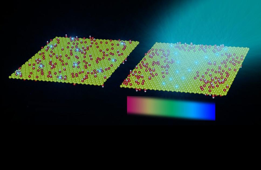
The low-temperature annealing process modifies the distribution of the oxygen atoms, causing them to form clusters and leaving areas of pure graphene between them, without introducing any disorder to the overall graphene structure — and most importantly, preserving the oxygen content.
Kumar says the new treatment allows the electrical resistance of the material to decrease by four to five orders of magnitude, which could be important for electronics, catalysis, and sensing applications. This is a result of the oxygen clustering, which renders the oxygen-rich regions insulating, but leaves the pure graphene areas in between conducting.
In addition, the pure graphene regions naturally have properties of “quantum dots”, which could find use as highly efficient light emitters, among other applications. The treatment also greatly enhances the material’s ability to absorb visible light, the team says. “It produces a 38 percent improvement in the collection of photons,” Grossman says, compared to untreated graphene oxide, “which is a significant improvement that could be important for its use in a number of applications, such as solar cells.”
While Grossman’s group is looking at the potential use of graphene in solar cells, thermoelectric devices, solar thermal fuels, and desalination filters, Belcher’s group is exploring biological applications, such as sensors for disease agents in the bloodstream, or delivery systems for targeting insoluble drugs to specific areas of the body.
The new processing approach, Grossman says, is “very exciting, because of how it opens up the design space for these applications.”
Given the great interest in graphene, “it is surprising that new processing regimes are still being identified,” says Mark Hersam, director of Northwestern University’s Materials Research Center, who was not involved in this work. This research “shows that there is still much work to be done on fully understanding and exploiting graphene,” he says.
The work, which included postdoc Sefaattin Tongay and associate professor Junqiao Wu at Berkeley, was supported by the Army Research Office, Eni, and the U.S. Department of Energy.
MIT team develops simple, inexpensive method that could help realize material’s promise for electronics, solar power, and sensors.
Publication Date:
Press Contact:

Caption:
Comparison of graphene oxide before (left) and after (right) the new annealing treatment. The graphene sheet is represented by yellow carbon spheres, while the oxygens and hydrogens are represented as red and white spheres. Annealing causes oxygen atoms to form clusters, creating areas of pure graphene (as shown in the right image). This results in increased light absorption, improved conduction of electrons, and efficient light emission.
Credits:
image: courtesy of the researchers


