MIT was named winner of the Software in Design Innovation Award at the Institution of Engineering and Technology’s (IET) Innovation Awards 2009 on Nov. 25 in London.
The IET Innovation Awards span 15 categories and attracted more than 300 entries from around the world. They represent a unique opportunity for innovators to be recognized and provide a showcase for the brightest ideas, highlighting the importance of innovation by celebrating its application across a range of engineering disciplines.
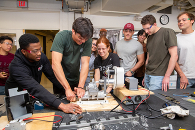
MIT’s winning team comprises Postdoctoral Associate Hayden Taylor and Professor Duane Boning, both from the Department of Electrical Engineering and Computer Science, as well as graduate students Matthew Dirckx and Eehern Wong of the Department of Mechanical Engineering.
Taylor and Boning have developed fast techniques for simulating two processes: the hot micro-embossing of thermoplastic polymeric materials, and nanoimprint lithography.
Thermoplastic micro-embossing is a low-cost, high-throughput technique for manufacturing polymeric ”lab-on-chip” microfluidic devices, which promise to bring reliable healthcare to every corner of the globe. Meanwhile, nanoimprint lithography is a revolutionary technique to slash the costs of semiconductor and data-storage manufacturing. In both processes, a patterned stamp mechanically deforms a layer of polymeric material, transferring a design to a product. Device designers need reassurance that any new pattern can be replicated with available apparatus. Conventionally, process development has been experimental and iterative, with engineers spending weeks in the lab and taking a substantial risk that the design itself will need to be changed — requiring a new stamp, at a cost of many tens of thousands of dollars for nanoimprint. The new simulation techniques developed at MIT offer a way of short-circuiting this wasteful development process.
Compared with conventional mechanical simulation techniques, such as finite element modeling, the new approach is at least 1,000 times faster. Using the techniques, engineers will be able to produce complex device designs that are amenable to imprinting or embossing, and select appropriate processing parameters before going into production.
The research was sponsored by the Singapore-MIT Alliance.
MIT’s entry to the competition described the simulation algorithms as well as exploring the commercial potential for nanoimprint-friendly semiconductor “design-for-manufacture” software based on the methods.
The IET is a professional organisation whose 150,000 members in 127 countries share and advance knowledge to promote science, engineering and technology across the world. For more information, visit http://www.theiet.org.
The IET Innovation Awards span 15 categories and attracted more than 300 entries from around the world. They represent a unique opportunity for innovators to be recognized and provide a showcase for the brightest ideas, highlighting the importance of innovation by celebrating its application across a range of engineering disciplines.
MIT’s winning team comprises Postdoctoral Associate Hayden Taylor and Professor Duane Boning, both from the Department of Electrical Engineering and Computer Science, as well as graduate students Matthew Dirckx and Eehern Wong of the Department of Mechanical Engineering.
Taylor and Boning have developed fast techniques for simulating two processes: the hot micro-embossing of thermoplastic polymeric materials, and nanoimprint lithography.
Thermoplastic micro-embossing is a low-cost, high-throughput technique for manufacturing polymeric ”lab-on-chip” microfluidic devices, which promise to bring reliable healthcare to every corner of the globe. Meanwhile, nanoimprint lithography is a revolutionary technique to slash the costs of semiconductor and data-storage manufacturing. In both processes, a patterned stamp mechanically deforms a layer of polymeric material, transferring a design to a product. Device designers need reassurance that any new pattern can be replicated with available apparatus. Conventionally, process development has been experimental and iterative, with engineers spending weeks in the lab and taking a substantial risk that the design itself will need to be changed — requiring a new stamp, at a cost of many tens of thousands of dollars for nanoimprint. The new simulation techniques developed at MIT offer a way of short-circuiting this wasteful development process.
Compared with conventional mechanical simulation techniques, such as finite element modeling, the new approach is at least 1,000 times faster. Using the techniques, engineers will be able to produce complex device designs that are amenable to imprinting or embossing, and select appropriate processing parameters before going into production.
The research was sponsored by the Singapore-MIT Alliance.
MIT’s entry to the competition described the simulation algorithms as well as exploring the commercial potential for nanoimprint-friendly semiconductor “design-for-manufacture” software based on the methods.
The IET is a professional organisation whose 150,000 members in 127 countries share and advance knowledge to promote science, engineering and technology across the world. For more information, visit http://www.theiet.org.