
Deblina Sarkar joins the MIT Media Lab faculty
New research group aims to bridge the gap between nanotechnology and synthetic biology.
New research group aims to bridge the gap between nanotechnology and synthetic biology.
A new study suggests a path to more efficient error correction, which may help make quantum computers and sensors more practical.

The mission of SENSE.nano is to foster the development and use of novel sensors, sensing systems, and sensing solutions.
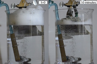
Bubbly buildup can hinder many industrial processes, but a new method can reduce or even eliminate it.
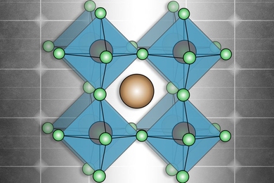
Starting with higher-value niche markets and then expanding could help perovskite-based solar panels become competitive with silicon.
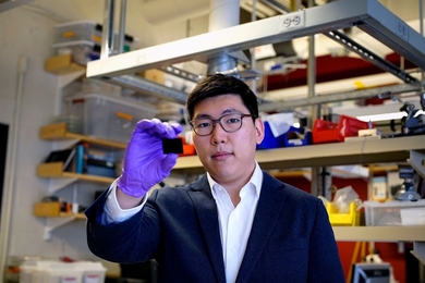
Next-generation devices made with new “peel and stack” method may include electronic chips worn on the skin.

An MIT team has devised a lithium metal anode that could improve the longevity and energy density of future batteries.

“Go Beyond” Award celebrates commitment to excellence in efficiency and sustainability.
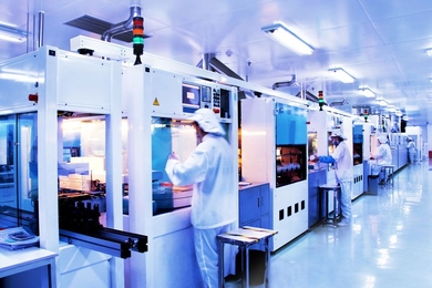
Solar panel costs have dropped lately, but slimming down silicon wafers could lead to even lower costs and faster industry expansion.
Assistant Professor Sili Deng is on a quest to understand the chemistry involved in combustion and develop strategies to make it cleaner.
Student committee puts together research showcase while balancing coursework, qualifying exams, and extracurriculars.

Professor of physics honored alongside Allan MacDonald and Rafi Bistritzer for pioneering research on twisted bilayer graphene.
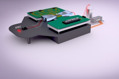
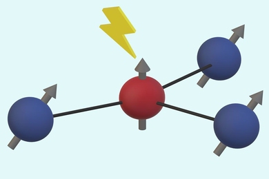
A new method determines whether circuits are accurately executing complex operations that classical computers can’t tackle.
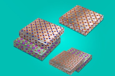
Carbon nanotube film produces aerospace-grade composites with no need for huge ovens or autoclaves.
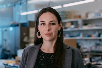
The MIT assistant professor is entranced by the beauty she finds pursuing chemistry.