
Have a damaged painting? Restore it in just hours with an AI-generated “mask”
A new method can physically restore original paintings using digitally constructed films, which can be removed if desired.
A new method can physically restore original paintings using digitally constructed films, which can be removed if desired.
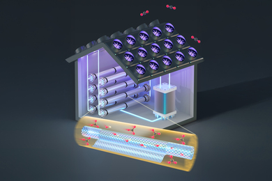
MIT engineers developed an atmospheric water harvester that produces fresh water anywhere — even Death Valley, California.
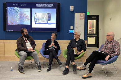
In the inaugural STUDIO.nano Resonance Lecture, the Brown University assistant professor traced how artists in the 1960s delved into early computer science, cybernetics, and AI.
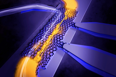
These devices could pack three times as much energy per pound as today’s best EV batteries, offering a lightweight option for powering trucks, planes, or ships.
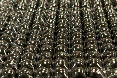
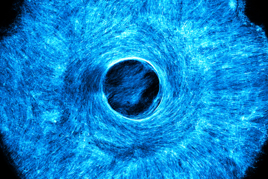
The “one-of-a-kind” phenomenon was observed in ordinary graphite.
Today’s carbon capture systems suffer a tradeoff between efficient capture and release, but a new approach developed at MIT can boost overall efficiency.

A new method could enable stretchable ceramics, glass, and metals, for tear-proof textiles or stretchy semiconductors.
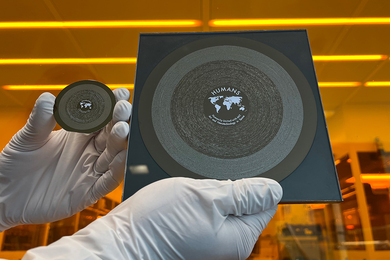
Professor Craig Carter’s precision design for a student-led project now on the moon encodes messages from around the world on a silicon wafer.

Connected by the MIT Human Insight Collaborative, Lecturer Mi-Eun Kim and Research Scientist Praneeth Namburi want to develop an understanding of musical expression and skill development.
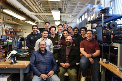
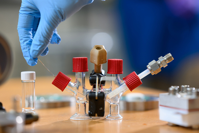
Inaugural cohort of Tecnológico de Monterrey undergraduates participate in immersive practicum at MIT featuring desktop fiber-extrusion devices, or FrEDs.
MIT engineers developed a way to grow artificial tissues that look and act like their natural counterparts.

Agreement between MIT Microsystems Technology Laboratories and GlobalFoundries aims to deliver power efficiencies for data centers and ultra-low power consumption for intelligent devices at the edge.

Rhombohedral graphene reveals new exotic interacting electron states.
By determining how readily electron pairs flow through this material, scientists have taken a big step toward understanding its remarkable properties.