
Unlocking ammonia as a fuel source for heavy industry
Four MIT alumni say their startup, Amogy, has the technology to help decarbonize maritime shipping, power generation, manufacturing, and more.
Four MIT alumni say their startup, Amogy, has the technology to help decarbonize maritime shipping, power generation, manufacturing, and more.

The team adapted the medical technique to study slag waste that was a byproduct of ancient copper smelting.

MIT.nano cleanroom complex named after Robert Noyce PhD ’53 at the 2025 Nano Summit.

Jacqueline Prawira’s innovation, featured on CBS’s “The Visioneers,” tackles one of the world’s most pressing environmental challenges.
Because it’s nearly impermeable to gases, the polymer coating developed by MIT engineers could be used to protect solar panels, machinery, infrastructure, and more.
The findings could open a route to new forms of higher-temperature superconductors.

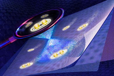
MIT researchers created microscopic wireless electronic devices that travel through blood and implant in target brain regions, where they provide electrical stimulation.

Adding amino acids to certain protein-based medications can improve stability and effectiveness. New MIT research demonstrates how it works.

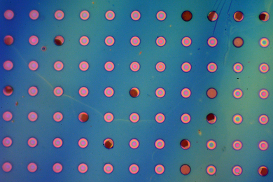
The DIGIT imaging tool could enable the design of quantum devices and shed light on atomic-scale processes in cells and tissues.

The newest MIT engineering faculty are conducting research across a diverse range of subject areas.

In a new study, MIT researchers evaluated quantum materials’ potential for scalable commercial success — and identified promising candidates.

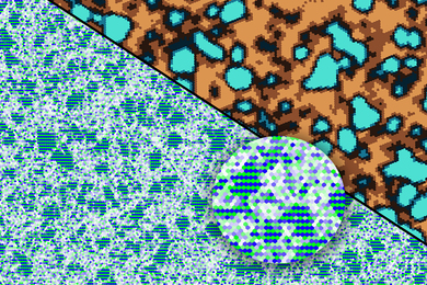
Acting as a “virtual spectrometer,” SpectroGen generates spectroscopic data in any modality, such as X-ray or infrared, to quickly assess a material’s quality.

MIT researchers discovered a hidden atomic order that persists in metals even after extreme processing.
Incorporating machine learning, MIT engineers developed a way to 3D print alloys that are much stronger than conventionally manufactured versions.
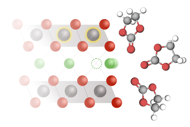
MIT researchers developed a model that explains lithium intercalation rates in lithium-ion batteries.